Thin film transistor, manufacturing method thereof, array substrate and display apparatus

A technology of thin film transistor and manufacturing method, which is applied in transistors, semiconductor/solid-state device manufacturing, electric solid-state devices and other directions, can solve problems such as affecting device stability and easily generating off-state current, so as to improve stability, improve display effect, The effect of reducing off-state current

Inactive Publication Date: 2018-06-01
HEFEI BOE DISPLAY TECH CO LTD +1
View PDF3 Cites 12 Cited by
  • Summary
  • Abstract
  • Description
  • Claims
  • Application Information

AI Technical Summary

Problems solved by technology

However, most of the current silicon-based semiconductors are sensitive to light, and it is easy to generate off-state current under light, which affects the stability of the device.

Method used


Image

  • Thin film transistor, manufacturing method thereof, array substrate and display apparatus
  • Thin film transistor, manufacturing method thereof, array substrate and display apparatus
  • Thin film transistor, manufacturing method thereof, array substrate and display apparatus

Examples


Embodiment Construction

[0052] Specific embodiments of the present invention will be described in detail below in conjunction with the accompanying drawings. It should be understood that the specific embodiments described here are only used to illustrate and explain the present invention, and are not intended to limit the present invention.

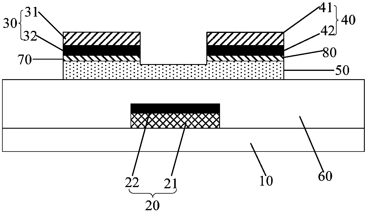
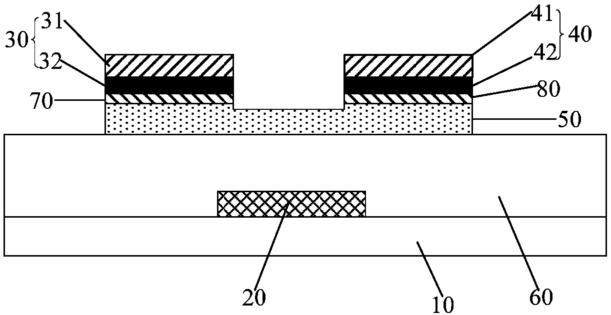
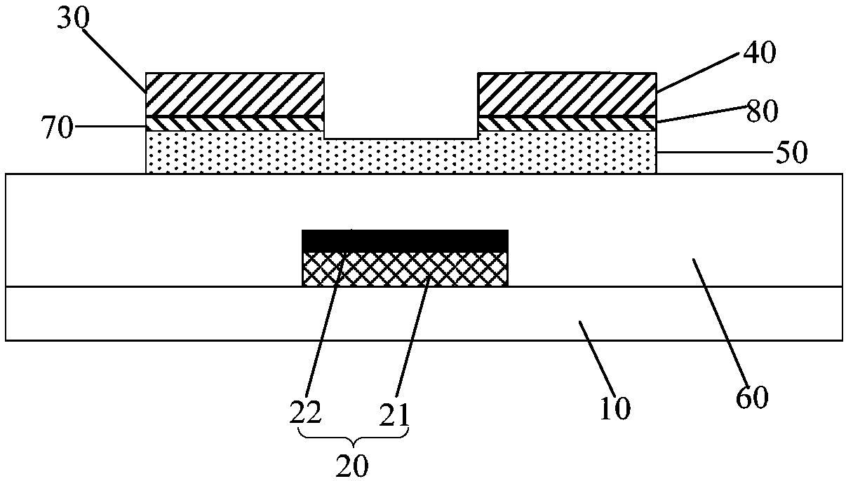
[0053] As an aspect of the present invention, a thin film transistor is provided, Figure 1 to Figure 6 Six structural schematic diagrams of thin film transistors are shown respectively, combined with Figure 1 to Figure 6 As shown, the thin film transistor includes a gate 20 , a source 30 , a drain 40 and an active layer 50 disposed on a substrate 10 , and both the source 30 and the drain 40 are electrically connected to the active layer 50 . At least one of the gate 20 , the source 30 and the drain 40 is a light-absorbing electrode, and the light-absorbing electrode includes an electrode body and a light-absorbing layer, and the light-absorbing layer is dispo...


PUM


Abstract

The invention provides a thin film transistor which comprises a grid electrode, a source electrode and a drain electrode arranged on a substrate and an active layer, the source electrode and the drainelectrode are electrically connected with the active layer, and at least one of the grid electrode, the source electrode and the drain electrode is a light absorption electrode. The light absorptionelectrode comprises an electrode body and a light absorption layer, the light absorption layer is arranged on one side, facing the active layer, of the electrode body. Correspondingly, the invention further provides a manufacturing method of the thin film transistor, an array substrate and a display device. The light irradiated on the active layer can be reduced, and the stability of the thin filmtransistor can be improved.

Description

technical field [0001] The invention relates to the field of semiconductor devices, in particular to a thin film transistor, a manufacturing method thereof, an array substrate and a display device. Background technique [0002] At present, amorphous silicon and low temperature polysilicon (LTPS) are widely used in semiconductor devices. However, most current silicon-based semiconductors are sensitive to light, and off-state currents are easily generated under light, which affects device stability. Contents of the invention [0003] The present invention aims to solve at least one of the technical problems existing in the prior art, and proposes a thin film transistor and its manufacturing method, an array substrate and a display device, so as to reduce the phenomenon that light hits the active layer and improve the stability of the thin film transistor. sex. [0004] In order to solve one of the above technical problems, the present invention provides a thin film transis...

Claims


Application Information

Patent Timeline
Patent Type & Authority Applications(China)
IPC IPC(8): H01L29/786H01L29/417H01L29/423H01L21/336H01L21/28H01L27/12
CPCH01L27/1214H01L29/401H01L29/41733H01L29/42384H01L29/6675H01L29/78663H01L29/78672H01L29/78633H01L27/1218H01L29/66742H01L29/7869
Inventor 张骥姜涛郭光龙高锦成惠官宝
Owner HEFEI BOE DISPLAY TECH CO LTD
Why Eureka
Try Eureka