Drive circuit for power semiconductor element, power conversion unit, and power conversion device
A technology of power semiconductors and drive circuits, which is applied in the direction of output power conversion devices, electrical components, electronic switches, etc., and can solve the problems of not being able to maximize the performance of power semiconductor components, limiting the number of parallel connections, and increasing costs.
- Summary
- Abstract
- Description
- Claims
- Application Information
AI Technical Summary
Problems solved by technology
Method used
Image
Examples
Embodiment approach
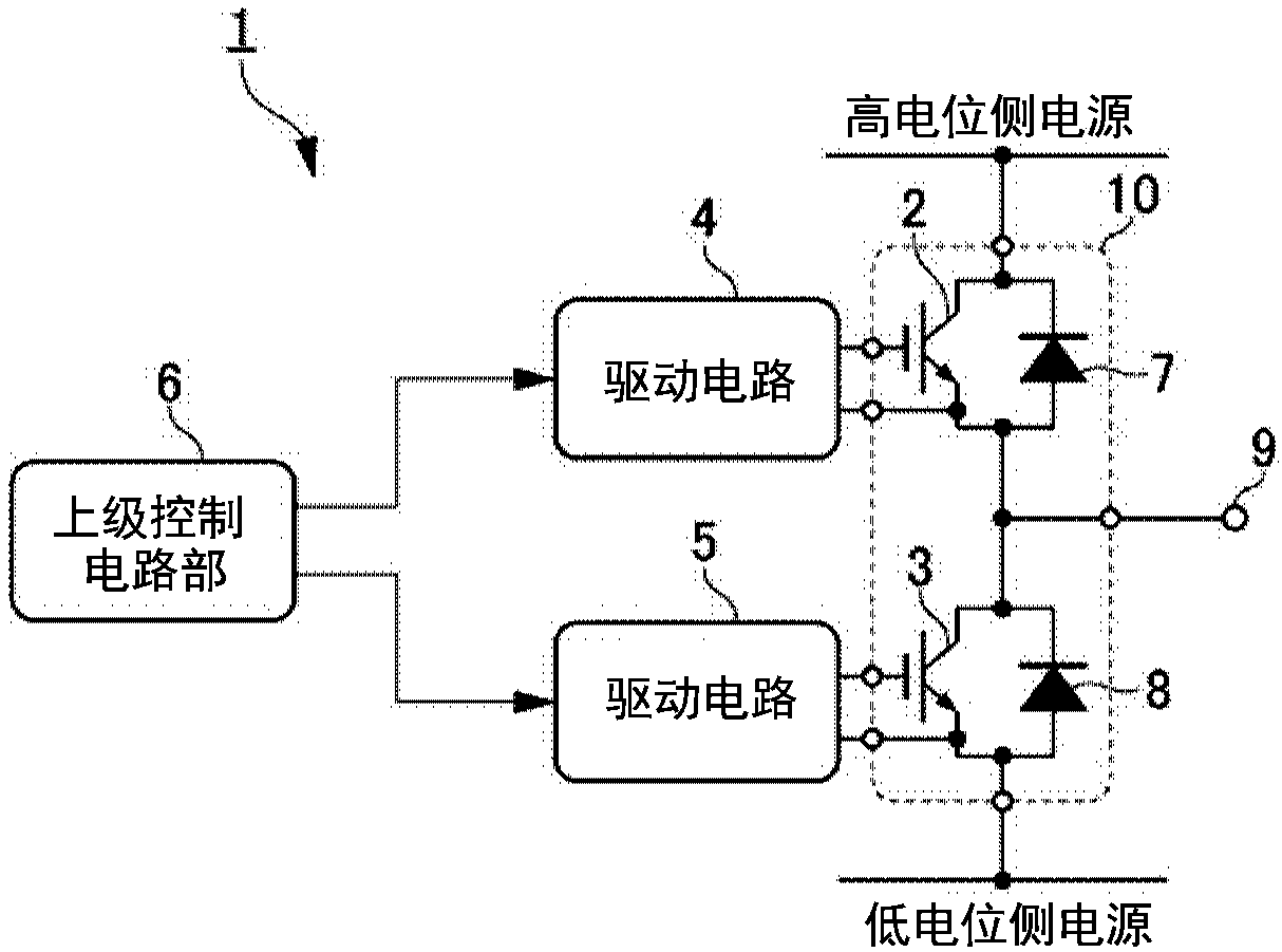
[0056] For this reason, in this embodiment, in figure 1 In the drive circuit 1 of the power semiconductor element shown, when the plurality of power semiconductor elements 2 and 3 connected in parallel are simultaneously driven to switch, the current fluctuations during the turn-on / off, that is, the switching operation and the steady-state operation are improved. balance. Here, the "steady-state operation" refers to the operation from after the power semiconductor elements 2 and 3 are turned on to before they are turned off, that is, the operation when the power semiconductor elements 2 and 3 are turned on.
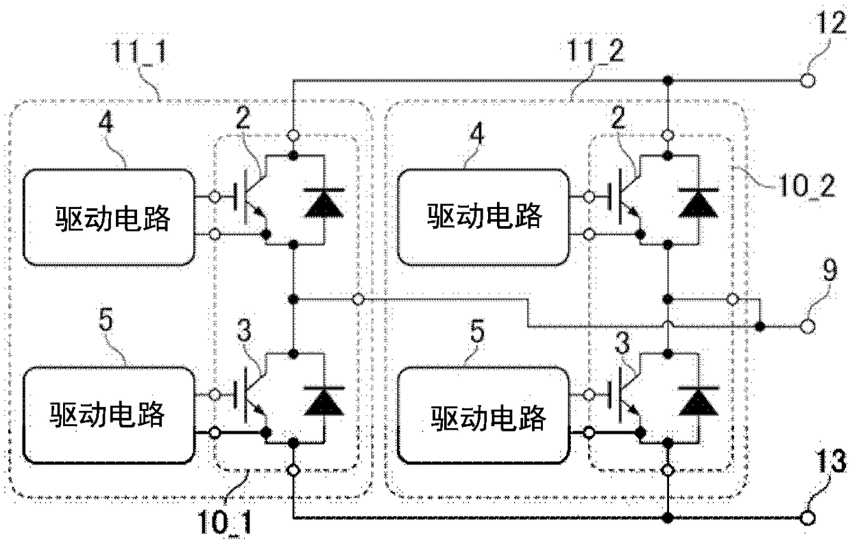
[0057] In the driving circuit 1 according to this embodiment, the power conversion modules 11 - 1 and 11 - 2 connected in parallel, and each of the upper arm driving circuit 4 and the lower arm driving circuit 5 provided corresponding to the plurality of power semiconductor elements 2 and 3 Both have a storage unit 51 for storing characteristic information of the power s...
Embodiment 1
[0062] Figure 4 This is an example of a block diagram showing the configuration of the power semiconductor element drive circuit 1 according to the first embodiment. The specific configuration of the lower arm drive circuit 5 of the power conversion units 11 - 1 and 11 - 2 will be described below, but the upper arm drive circuit 4 also has the same configuration. The lower arm drive circuit 5 (hereinafter simply referred to as "drive circuit 5") includes a storage unit (storage device) 51, an interface (I / F) circuit unit 52, a delay circuit unit 53, a gate voltage gradient variable circuit unit 54, and Gate voltage variable circuit section 55 .
[0063] The storage unit 51 stores characteristic information of the lower arm power semiconductor element 3 . The information stored in the storage unit 51 is preferably, for example, information on a characteristic distribution map of each power semiconductor element acquired at the time of shipment inspection of the power semicon...
Embodiment 2
[0076] Example 2 is a modified example of Example 1. Figure 8 This is an example of a block diagram showing the configuration of a drive circuit 1 for a power semiconductor element according to the second embodiment. Such as Figure 8 As shown, the driving circuit 1 of the power semiconductor element according to the second embodiment includes current sensors 61-1, 61-2 and a current calculation circuit in addition to the components of the driving circuit 1 of the power semiconductor element according to the first embodiment. The configuration of the parts 62-1 and 62-2.
[0077] Current sensors 61 - 1 and 61 - 2 detect information corresponding to currents flowing through power semiconductor elements 2 and 3 . Current calculation units 62-1 and 62-2 calculate currents actually flowing through power semiconductor elements 2 and 3 based on detection outputs (detection information) of current sensors 61-1 and 61-2. In this example, the current sensors 61 - 1 and 61 - 2 and t...
PUM
 Abstract
Description
Claims
Application Information


