Drive circuit for power semiconductor element, power conversion module, and power conversion device

A technology for power semiconductors and driving circuits, which is applied to output power conversion devices, electrical components, electronic switches, etc., and can solve problems such as the limitation of the number of parallel connections, the inability to maximize the performance of power semiconductor components, and the increase in cost.

Active Publication Date: 2020-02-18
HITACHI LTD
View PDF4 Cites 0 Cited by
  • Summary
  • Abstract
  • Description
  • Claims
  • Application Information

AI Technical Summary

Problems solved by technology

For this reason, the performance of power semiconductor components cannot be maximized
[0004] In addition, by selecting power semiconductor elements and combining power semiconductor elements with the same characteristics, the above-mentioned problems can be solved, but the increase in cost and the limitation of the number of parallel connections when selecting characteristics are problems.

Method used


Image

  • Drive circuit for power semiconductor element, power conversion module, and power conversion device
  • Drive circuit for power semiconductor element, power conversion module, and power conversion device
  • Drive circuit for power semiconductor element, power conversion module, and power conversion device

Examples


Embodiment approach

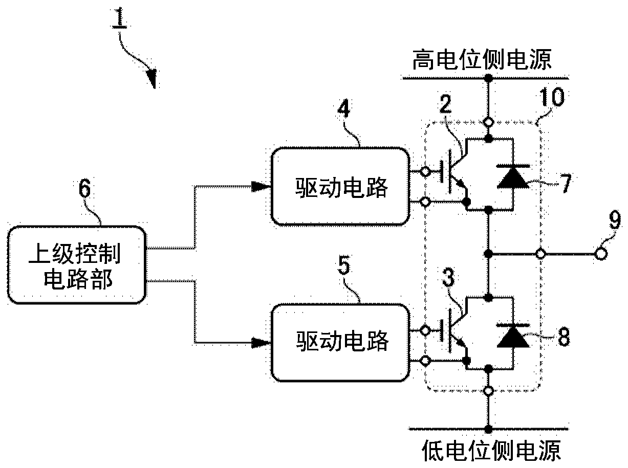
[0056] Therefore, in this embodiment, the figure 1 In the drive circuit 1 of the power semiconductor element shown, when the plurality of power semiconductor elements 2 and 3 connected in parallel are simultaneously switched and driven, the current variation at the time of on / off, that is, the switching operation and the steady-state operation is improved. balance. Here, the "steady-state operation" refers to the operation during the period from after the power semiconductor elements 2 and 3 are turned on and before the power semiconductor element 3 is turned off, that is, the operation when the power semiconductor elements 2 and 3 are turned on.

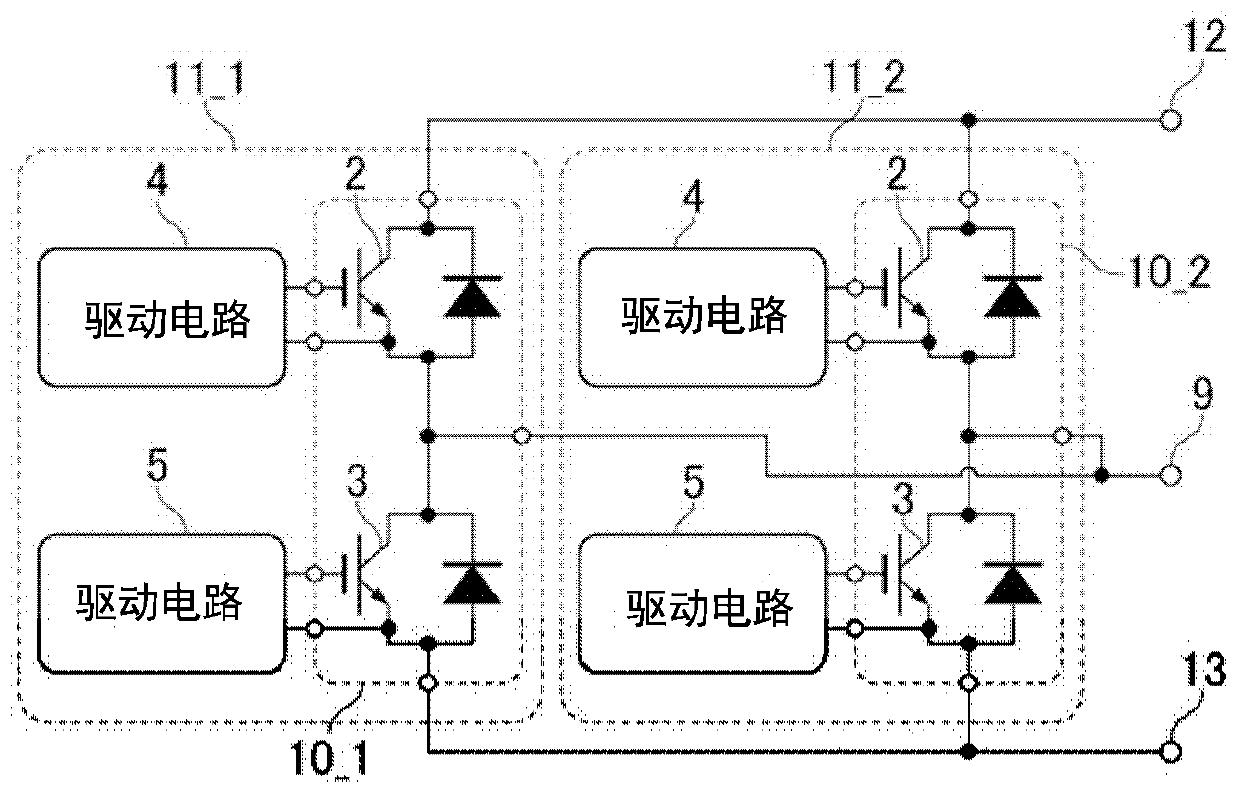
[0057] In the drive circuit 1 according to the present embodiment, the power conversion modules 11 - 1 and 11 - 2 connected in parallel are connected to each of the upper arm drive circuit 4 and the lower arm drive circuit 5 provided corresponding to the plurality of power semiconductor elements 2 and 3 . Either one has a storage u...

Embodiment 1

[0062] Figure 4 This is an example of a block diagram showing the configuration of the drive circuit 1 of the power semiconductor element according to the first embodiment. The specific configuration of the lower arm drive circuit 5 of the power conversion modules 11-1 and 11-2 will be described below, but the upper arm drive circuit 4 also has the same configuration. The lower arm drive circuit 5 (hereinafter simply referred to as “drive circuit 5 ”) includes a storage unit (storage device) 51 , an interface (I / F) circuit unit 52 , a delay circuit unit 53 , a gate voltage slope variable circuit unit 54 , and The gate voltage variable circuit unit 55 .

[0063] The storage unit 51 stores characteristic information of the lower arm power semiconductor element 3 . As the information to be stored in the storage unit 51 , for example, it is preferable that the information of the characteristic distribution map of each power semiconductor element acquired at the time of shipping...

Embodiment 2

[0076] Example 2 is a modification of Example 1. Figure 8 This is an example of a block diagram showing the configuration of the drive circuit 1 of the power semiconductor element according to the second embodiment. like Figure 8 As shown, the drive circuit 1 of the power semiconductor element according to the second embodiment includes current sensors 61-1 and 61-2, and a current calculator in addition to the constituent elements of the power semiconductor element drive circuit 1 according to the first embodiment. The configuration of the parts 62-1 and 62-2.

[0077] The current sensors 61 - 1 and 61 - 2 detect information according to currents flowing through the power semiconductor elements 2 and 3 . The current calculation units 62-1 and 62-2 calculate the currents actually flowing through the power semiconductor elements 2 and 3 based on the detection outputs (detection information) of the current sensors 61-1 and 61-2. In this example, the current sensors 61 - 1 an...


PUM


Abstract

The drive circuit for a power semiconductor element according to the present invention is a drive circuit provided corresponding to a plurality of power semiconductor elements connected in parallel to drive the power semiconductor element. Furthermore, the driving circuit of the power semiconductor element of the present invention includes: a storage unit storing characteristic information of the power semiconductor element; and a gate drive control unit controlling gate driving conditions of the power semiconductor element based on the characteristic information stored in the storage unit.

Description

technical field [0001] The present invention relates to a drive circuit of a power semiconductor element, a power conversion module, and a power conversion device. Background technique [0002] As the power conversion device, there are an inverter device for converting DC power into AC power, and a converter device for converting AC power into DC power. In these power conversion devices, although power conversion is performed by switching operation of power semiconductor elements, a plurality of power semiconductor elements are connected in parallel for the purpose of increasing the converted power capacity, and the plurality of power semiconductor elements are simultaneously switched and driven. . [0003] When a plurality of power semiconductor elements are connected in parallel and driven in this way, there is a variation in element-specific characteristics such as threshold voltage and turn-on voltage among the power semiconductor elements, so that when these power semi...

Claims


Application Information

Patent Timeline
Patent Type & Authority Patents(China)
IPC IPC(8): H02M1/08H02M1/00H03K17/08H03K17/12H03K17/567
CPCH02M1/08H03K17/08H03K17/12H03K17/56
Inventor 三间彬
Owner HITACHI LTD
Why Eureka
Try Eureka