Power conversion device and power semiconductor element control method

A power conversion device and power semiconductor technology, which is applied in the direction of output power conversion devices and electrical components, can solve problems such as insufficient current imbalance and characteristic deviation of power semiconductor components, and achieve improvement of current imbalance and improvement of current imbalance , the effect of increasing the number of connections

Active Publication Date: 2018-05-25
HITACHI LTD
View PDF5 Cites 0 Cited by
  • Summary
  • Abstract
  • Description
  • Claims
  • Application Information

AI Technical Summary

Problems solved by technology

[0014] The methods for solving the problem of variation in the characteristics of power semiconductor elements described in the above-mentioned Patent Documents 1 and 2 do not sufficiently improve the current imbalance.

Method used


Image

  • Power conversion device and power semiconductor element control method
  • Power conversion device and power semiconductor element control method
  • Power conversion device and power semiconductor element control method

Examples


Embodiment Construction

[0033] Hereinafter, an embodiment example (hereinafter referred to as "this example") of the present invention will be described with reference to the drawings.

[0034] [1. Example of element control structure of power conversion device]

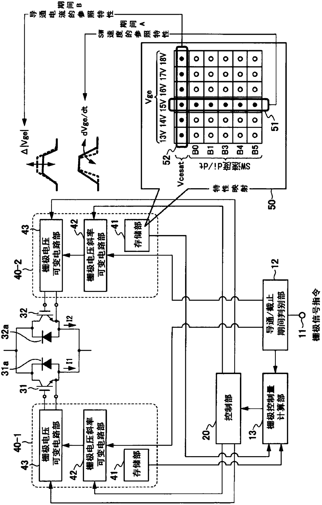
[0035] figure 1 An example of a drive circuit for controlling elements of the power conversion device of this example and its peripheral configuration is shown.

[0036] figure 1 The structure of two power semiconductor elements 31 and 32 connected in parallel and the drive circuits 40-1 and 40-2 of each power semiconductor element 31 and 32 is shown in the figure. As will be described later, a power conversion device generally has a structure in which a plurality of power semiconductor elements are connected in parallel, but here an example of two power semiconductor elements 31 and 32 is shown for simplification of description.

[0037] As the power semiconductor elements 31 and 32 , for example, insulated gate bipolar transistors (IGB...


PUM


Abstract

The invention solves the problem caused by variations in power semiconductor elements connected in parallel and provided in the power conversion device. The power semiconductor device includes a determination unit for determining the duration time of the on state of the gate signal of the power semiconductor element, a storage unit for storing the characteristics of the power conversion element ofeach power semiconductor element, and a control unit that performs equalization control of switching speed and equalization control of conduction current of each power semiconductor element. The control unit performs equalization control of the switching speed of each power semiconductor element based on the characteristics of the power conversion element stored in the storage unit, and performsequalization control of the conduction current of each power semiconductor element based on the characteristics of the power conversion element stored in the storage unit when the determination unit determines that the on state continues for a predetermined time or more.

Description

technical field [0001] The invention relates to a rate conversion device and a control method for a power semiconductor element. Background technique [0002] In recent years, inverter devices used as power conversion devices for converting DC power to AC power, or AC power to DC power, have been required to have higher output densities, and have been reduced in size and weight. In particular, as the miniaturization of power conversion units integrated with components such as power semiconductor modules, capacitors, and bus bars on which power semiconductor elements are mounted, miniaturization and cost reduction of drive circuits for driving power semiconductor elements demand continues to increase. [0003] In addition, by installing multiple power conversion units that integrate components such as power semiconductor modules, capacitors, bus bars, and gate drive circuits, we strive to achieve common use of components and increase output capacity, thereby realizing the po...

Claims


Application Information

Patent Timeline
Patent Type & Authority Applications(China)
IPC IPC(8): H02M1/088
CPCH02M1/088
Inventor 三间彬森和久松元大辅上妻央
Owner HITACHI LTD
Why Eureka
Try Eureka