Switching semiconductor device parallel circuit and control method thereof

A semiconductor and device technology, applied in the field of parallel connection of switching semiconductor devices, can solve the problems of inability to significantly reduce the voltage change rate of the switch tube, increase the voltage change rate, and the switching loss of the parallel switch tube is large, so as to reduce the switching loss and reduce the dv /dt noise, to achieve the effect of current sharing

Active Publication Date: 2021-01-05
申彦峰 +2
View PDF17 Cites 0 Cited by
  • Summary
  • Abstract
  • Description
  • Claims
  • Application Information

AI Technical Summary

Problems solved by technology

[0005] Although the above methods can improve the current sharing characteristics of the parallel switching tubes, in hard switching applications, the switching loss of the parallel switching tubes is still large
Moreover, due to the fast switching speed, the voltage change rate (dv / dt noise) of the wide bandgap semiconductor switch tube is significantly higher than that of the silicon semiconductor switch tube, which poses a greater challenge to the electromagnetic compatibility of the power electronic system
However, the existing wide bandgap semiconductor switch tube parallel connection scheme cannot significantly reduce the voltage change rate (dv / dt) of the switch tube

Method used


Image

  • Switching semiconductor device parallel circuit and control method thereof
  • Switching semiconductor device parallel circuit and control method thereof
  • Switching semiconductor device parallel circuit and control method thereof

Examples


Embodiment Construction

[0036] Specific embodiments of the present invention will be described in detail below in conjunction with the accompanying drawings.

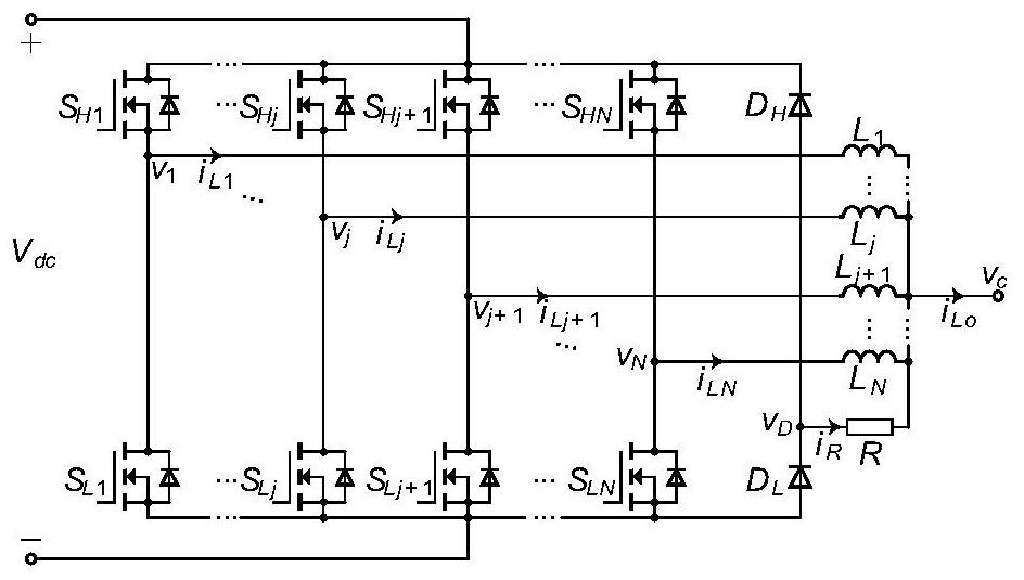
[0037] Such as figure 1 The parallel circuit of power switching semiconductor devices is shown, including the DC bus V dc The positive and negative terminals, the output terminal v c , the first upper bridge arm switch tube S H1 , the second upper bridge arm switching tube S H2 ,..., the Nth (N≥2) upper bridge arm switch tube S HN , the first lower bridge arm switch tube S L1 , the second lower bridge arm switch tube S L2 ,..., Nth lower bridge arm switch tube S LN , the first commutation inductance L 1 , the second commutation inductance L 2 ,..., Nth commutation inductance L N , High-side diode D H Lower arm diode DL and damping resistor R.

[0038] Among them, the first upper bridge arm switch S H1 The source of the first lower bridge arm switch S L1 The drain connection of the first switching tube bridge arm and the second upp...


PUM


Abstract

The invention discloses a power switch semiconductor device parallel circuit, N commutation inductors are connected to the midpoints of N power switch semiconductor device half-bridges connected in parallel, and all the commutation inductors are connected to an output terminal and are connected with the midpoints of power diode half-bridges through damping resistors. The N power switch semiconductor device half-bridges are divided into two groups of main bridge arms and auxiliary bridge arms, and the auxiliary bridge arms are turned on before the main bridge arms are turned on, so that all power switch tubes of the main bridge arms realize zero-voltage turn-on, the auxiliary bridge arm switch tubes realize zero-voltage or zero-current turn-on, and the turn-on loss of the power switch tubesis remarkably reduced. Resonance is carried out by utilizing a commutation inductor and a parasitic output capacitor of a diode, so that slow change of the voltage of an output terminal is realized,and dv/dt of the output voltage is remarkably reduced. The invention further discloses a working method of the circuit.

Description

technical field [0001] The invention belongs to the technical field of power electronics, and in particular relates to a parallel connection technology of switching semiconductor devices. Background technique [0002] In recent years, renewable energy and electric vehicles are gradually replacing traditional fossil energy and vehicles. The realization of this energy change requires high-efficiency and high-power-density power electronic converters. As the main components of power electronic converters, the market share of power switching semiconductor devices is constantly increasing. In particular, as the wide bandgap power switching semiconductor device technology continues to mature, its switching characteristics and reliability continue to improve. However, due to yield, thermal management, and cost constraints, the current ratings of wide-bandgap semiconductor die and discrete devices are still relatively low, as published in IEEE Transactions on Power Electronics Vol....

Claims


Application Information

Patent Timeline
Patent Type & Authority Applications(China)
IPC IPC(8): H02M1/00H02M7/5387
CPCH02M1/00H02M7/5387H02M1/0058Y02B70/10
Inventor 申彦峰龙腾赵晖
Owner 申彦峰
Why Eureka
Try Eureka