Power conversion device

A power conversion device and current technology, applied in the direction of output power conversion devices, electrical components, electronic switches, etc., can solve the problem of not reducing the dv/dt noise of the power conversion device, and achieve the optimization and reduction of power loss and noise noise effect

Pending Publication Date: 2021-07-23
FUJI ELECTRIC CO LTD
View PDF2 Cites 0 Cited by
  • Summary
  • Abstract
  • Description
  • Claims
  • Application Information

AI Technical Summary

Problems solved by technology

However, the above-mentioned Patent Document 1 does not reduce dv / dt noise when the power conversion device operates in a small current region

Method used


Image

  • Power conversion device
  • Power conversion device
  • Power conversion device

Examples


no. 1 approach

[0068] (constitute)

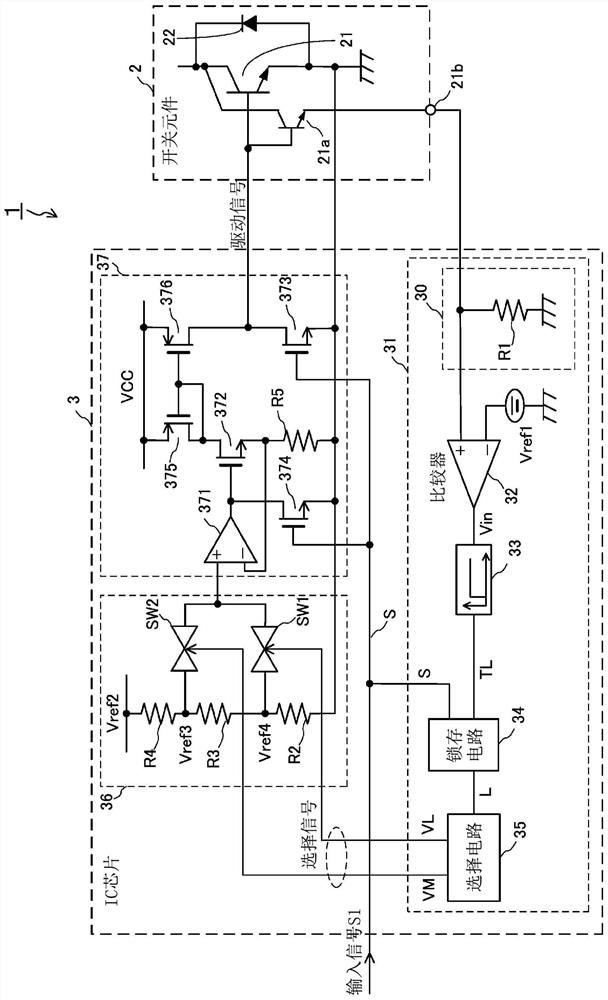
[0069] The IPM (Intelligent Power Module) 1 of this embodiment is suitable for, for example, joints of industrial robots, elevators, or power conversion devices for commercial air conditioners, such as figure 1 As shown, the configuration mainly includes a switching element 2 and an IC chip 3 .

[0070] The switching element 2 may be composed of, for example, an IGBT 21 and a freewheel diode 22 connected in antiparallel to the IGBT 21 , and may be a one-chip RC-IGBT. The IGBT 21 is turned on by a drive signal applied from the IC chip 3 to the gate (control electrode terminal), and a current (main current) flows from the collector to the emitter to supply constant power to a load not shown. The emitter of IGBT21 is connected to the reference potential of IC chip 3 mentioned later. Moreover, IGBT21a for current sensing is connected in parallel with IGBT21, and outputs a sense current at a fixed ratio according to a main current.

[0071] The IC chip 3 i...

no. 2 approach

[0110] Next, a second embodiment will be described.

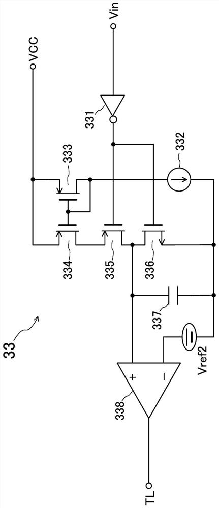
[0111] Image 6 It is a configuration diagram of the power conversion device of the second embodiment. and figure 1 The difference is that the constant current source 38 is provided on the side of the connection point of the resistance element R1 that converts the sense current into a voltage, and the sense terminal 21b. Otherwise with figure 1 are the same, and therefore the same elements are attached with the same symbols and descriptions thereof are omitted.

[0112] The constant current output from the constant current source 38 flows to the reference potential through the resistance element R1. Thus, the sensing voltage value increases by the amount of voltage generated by the constant current value and the resistance value of the resistance element R1.

[0113] Actually, about 10% of the rated current of the IGBT is sometimes specified as a small current range. In this case, to figure 1 When the low current ...

no. 3 approach

[0119] Next, a third embodiment will be described.

[0120] Figure 8 It is a configuration diagram of the power conversion device of the third embodiment. and figure 1 The difference is that constant current sources and P-type A series circuit of MOSFETs.

[0121] Hereinafter, the configuration of this embodiment will be described in detail.

[0122] exist Figure 8 Among them, the source of the P-type MOSFET 377 is connected to the output terminal of the constant current source 39 and the non-inverting input terminal of the comparator 32 . The drain of the P-type MOSFET 377 is connected to the reference potential. The gate of the P-type MOSFET 377 is connected to one end of the resistance element R1 and the sensing terminal 21b. The other end of the resistance element R1 is connected to a reference potential.

[0123] In addition, the source of the P-type MOSFET 378 is connected to the output terminal of the constant current source 40 and the inverting input terminal ...


PUM


Abstract

This power conversion device is provided with: a semiconductor switching element that has a control electrode terminal and two main electrode terminals and controls a current flowing between the two main electrode terminals by means of a drive signal applied to the control electrode terminal; and a drive circuit that generates the drive signal in synchronization with an input signal and turns on / off the semiconductor switching element by means of the drive signal, wherein the drive circuit detects the current flowing between the two main electrodes at a timing when the semiconductor switching element is turned off, and reduces the drive capacity when the detected current reaches a certain value or less. Accordingly, dv / dt noise, when the semiconductor switching element that operates in a relatively small current region is switched, is reduced.

Description

technical field [0001] The present invention relates to a power conversion device including a semiconductor switching element, and more particularly, to a power conversion device that adjusts the drive capability of the semiconductor switching element based on an output current of the power conversion device. Background technique [0002] Conventionally, there have been proposed techniques for reducing noise generated by switching operations of semiconductor switching elements such as IGBTs constituting a power conversion device. [0003] For example, Patent Document 1 discloses a switching element driving device that turns on an upper arm MOS transistor with a high driving capability, and then turns on the MOS transistor when the output current of the MOS transistor reaches the output current of the previous switching. The lowering of the driving capability of the MOS transistor moderates the change rate of the reverse recovery current of the freewheeling diode of the lower...

Claims


Application Information

Patent Timeline
Patent Type & Authority Applications(China)
IPC IPC(8): H02M1/08H03K17/16H03K17/567
CPCH02M1/08H03K17/16H03K17/567H02M1/44H03K17/165H03K17/0412H02M1/088H03K17/08116H03K17/161H03K2217/0027
Inventor 中森昭
Owner FUJI ELECTRIC CO LTD
Why Eureka
Try Eureka