
A method for preparing a multi-channel narrowband filter pixel array

A pixel array and narrow-band filter technology, which is applied in the field of preparation of multi-channel narrow-band filter pixel arrays, can solve the problems of unmatched pixel matching, difficult performance guarantee, low spectral sensitivity, etc., and achieves flexible design, graphic realization, and simple process Effect

Active Publication Date: 2020-07-03
湖南宏动光电有限公司
View PDF5 Cites 0 Cited by
  • Summary
  • Abstract
  • Description
  • Claims
  • Application Information

AI Technical Summary

Problems solved by technology

The disadvantage is that its spectral sensitivity is low, generally greater than 10nm; moreover, the more filtering channels, the more complex the process, and the edge of the narrow-band filtering unit corresponding to the CCD pixel is easily affected by the process, and cannot be completely matched with the pixel. Difficult to guarantee

Method used


Image

  • A method for preparing a multi-channel narrowband filter pixel array
  • A method for preparing a multi-channel narrowband filter pixel array
  • A method for preparing a multi-channel narrowband filter pixel array

Examples


preparation example Construction

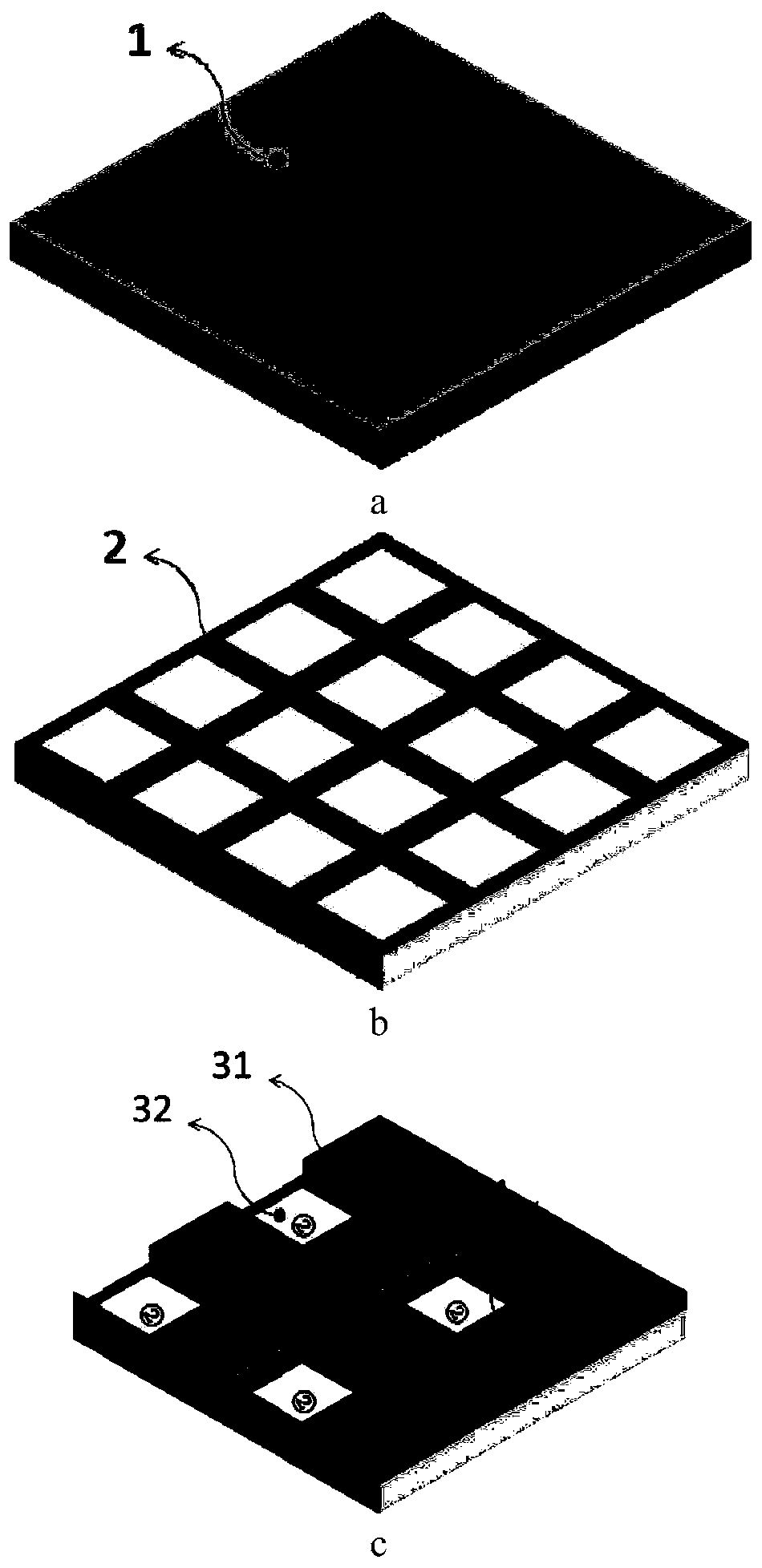
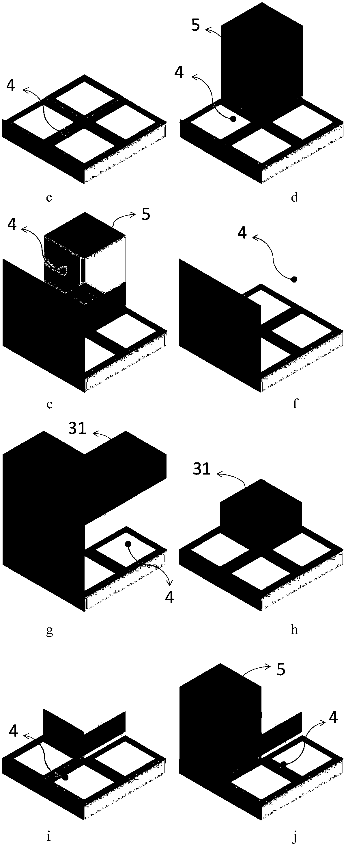
[0042] A method for preparing a multi-channel narrowband filter pixel array, comprising the steps of:

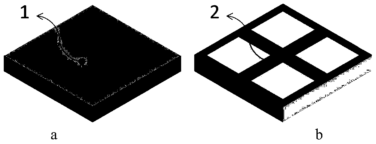
[0043] Step 1, using ultraviolet lithography and electron beam evaporation coating processes on the substrate to fabricate overlay marks and metal light-shielding grids between periodic filter pixel units;

[0044] Step 2, making a layer of metal aluminum conductive film on the surface of the substrate by ultraviolet lithography and electron beam evaporation coating as the starting substrate for electroplating;

[0045] Step 3, forming a photoresist mask by ultraviolet lithography;

[0046] Step 4, putting the substrate on which the photoresist pattern has been made into the electroplating solution pool for electroplating;

[0047] Step 5, removing the photoresist mask, and corroding the metal aluminum conductive film on the surface of the substrate to form an aluminum mask;

[0048] Step 6, using ion sputtering coating method to prepare F-P type periodic interference film...


PUM

PropertyMeasurementUnit
Sensitivityaaaaaaaaaa
wavelengthaaaaaaaaaa

Abstract

A method for preparing a multichannel narrow-band filtering pixel array includes the following steps: 1, manufacturing alignment marks and metal louvers on a substrate; 2, manufacturing a metallic aluminium conductive thin film on the surface of the substrate as an initial substrate of electroplating; 3, forming a photoresist mask through ultraviolet lithography; 4, putting the substrate on whicha photoresist pattern is manufactured in an electroplating liquid tank to be electroplated; 5, removing the photoresist mask and corroding the metallic aluminium conductive thin film on the surface ofthe substrate, and forming an aluminium mask; 6, adopting an ion sputtering coating method to prepare an F-P type periodical interference film system with specific optical characteristics; 7, corroding the aluminium mask, and forming a narrow-band filtering pixel array of a first channel; repeating Steps 2 to 7 to complete preparation of pixel arrays of second, third and fourth channels in sequence; and 9, performing bonding packaging on multichannel micro optical filters and a CCD detector. While maintaining characteristics of an optical thin film, the method provided by the invention realizes patterning of a large-thickness optical thin film, has a simple and reliable manufacturing process, facilitates popularization, and has relatively high practical value.

Description

technical field [0001] The invention relates to the fields of optical film preparation, optical micro-device preparation, nanophotonics and remote sensing detection, and in particular to a preparation method of a multi-channel narrow-band filter pixel array, which has F-P periodic multilayer dielectric film narrow-band micro-arrays with different working wavelengths. The filter performs multi-channel narrow-band filtering, which can be applied to spectral imaging. Background technique [0002] In the late 1970s and early 1980s, on the basis of studying and summarizing the spectral characteristics of various ground objects, everyone gradually realized that if continuous narrow-band imaging can be realized, then it is possible to realize the direct identification of ground minerals, resulting in the spectral Imaging spectroscopy technology combined with images. In 1983, the Jet Propulsion Laboratory of the United States developed the first airborne imaging spectrometer (AIS-1...

Claims


Application Information

Patent Timeline
Patent Type & Authority Patents(China)
IPC IPC(8): G02B5/28G01J3/02
CPCG01J3/0205G02B5/285
Inventor 唐文江
Owner 湖南宏动光电有限公司
Learn More