Method for processing excess tape of communication IC metal-based carrier board

A technology of metal base and carrier board, which is applied in the cleaning/polishing, photolithography/patterning, patterning and photolithography of conductive patterns, etc., to achieve the effect of reducing the scrap rate

Inactive Publication Date: 2018-06-26
WUXI SHENNAN CIRCUITS CO LTD
View PDF4 Cites 0 Cited by
  • Summary
  • Abstract
  • Description
  • Claims
  • Application Information

AI Technical Summary

Problems solved by technology

[0003] The purpose of the present invention is to provide a method for solving the residual glue on IC metal-based carrier boards for communication, so as to solve the technical problem of removing PP dust and residual glue at the bottom by manual grinding in the industry in the prior art

Method used


Image

  • Method for processing excess tape of communication IC metal-based carrier board

Examples


Embodiment Construction

[0019] Embodiments of the present invention will be described in detail below in conjunction with the accompanying drawings.

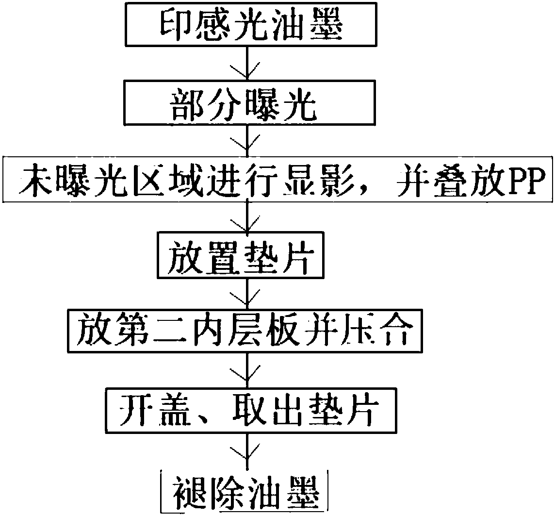
[0020] see figure 1 , the preferred embodiment of the present invention provides a kind of method for solving the residual glue of IC metal-based carrier board used for communication, comprising the following steps: then exposing the ink in the region that needs to be grooved on the first inner layer board, so that the ink occurs Optical reaction; then developing the ink in the unexposed area on the first inner layer plate to remove the ink through a chemical reaction, removing the ink in the unexposed area through a chemical reaction, and stacking PP on the developed area, Make the PP powder produced during the pressing process fall on the ink; then place a gasket in the area where the PP is not stacked, and play a supporting role in the second inner layer board pressing process; then place the PP and the gasket Place the second inner layer board on ...


PUM


Abstract

The invention discloses a method for processing the excess tape of a communication IC metal-based carrier board. The method comprises steps that firstly, the first inner board is entirely printed withphotosensitive ink; secondly, the ink of a grooving area of the first inner plate is exposed; thirdly, the ink of an unexposed area of the first inner plate is developed to remove the ink; fourthly,the PP is stacked at the area after development, and a gasket is arranged at the area without the PP; fifthly, a second inner plate is arranged at an upper surface of the PP and the gasket, and high temperature stitching is carried out; the second inner plate after stitching is opened, and the gasket is taken out; after the gasket is taken out, the ink is removed. The method is advantaged in thatthe first inner plate is printed with the ink for protection, both the PP powder and the PP residual tape drop on the ink in the whole stacking and stitching process, only through removing the ink, the PP powder and the PP excess tape disappear naturally, and manual grinding is not needed.

Description

technical field [0001] The invention relates to the technical field of processing IC metal-based carrier boards for communication, and in particular, relates to a method for solving residual glue on IC metal-based carrier boards for communication. Background technique [0002] The high-density IC substrate for high-end semiconductor communication is an essential component for the mutual conversion between optical transmission signals and electrical transmission signals in optical communication networks. The high-end carrier board factory is monopolized, and the price is very expensive; this product uses a metal base for high-power heat dissipation, and this process needs to add gaskets during the processing. A lot of dust falls on the bottom of the steps. After pressing, the dust and residual glue are cured and left behind. At present, manual grinding is used in the industry to remove the bottom PP dust and residual glue. However, this method requires a lot of manpower , an...

Claims


Application Information

Patent Timeline
Patent Type & Authority Applications(China)
IPC IPC(8): H05K3/26
CPCH05K3/26H05K2203/0502H05K2203/17
Inventor 徐明焦云峰
Owner WUXI SHENNAN CIRCUITS CO LTD
Why Eureka
Try Eureka