Chip embedding device

A technology of embedding devices and chips, applied in projection devices, optics, instruments, etc., can solve problems such as volume, heat dissipation, stability, etc., and achieve the effects of high stability, small volume, and high heat dissipation

Pending Publication Date: 2018-06-29
SHENZHEN ORBBEC CO LTD
View PDF6 Cites 3 Cited by
  • Summary
  • Abstract
  • Description
  • Claims
  • Application Information

AI Technical Summary

Problems solved by technology

[0005] In order to solve the problems of volume, heat dissipation and stability in the field of combining chips and circuit boards in the prior art, the present invention provides a chip embedding device

Method used


Image

  • Chip embedding device
  • Chip embedding device
  • Chip embedding device

Examples


Embodiment Construction

[0019] The present invention will be described in detail below through specific embodiments in conjunction with the accompanying drawings, so as to better understand the present invention, but the following embodiments do not limit the scope of the present invention. In addition, it should be noted that the diagrams provided in the following embodiments are only schematically illustrating the basic concept of the present invention, and only the components related to the present invention are shown in the drawings rather than the number of components, Shape and size drawing, the shape, quantity and proportion of each component can be changed arbitrarily during actual implementation, and the layout of the components may also be more complex.

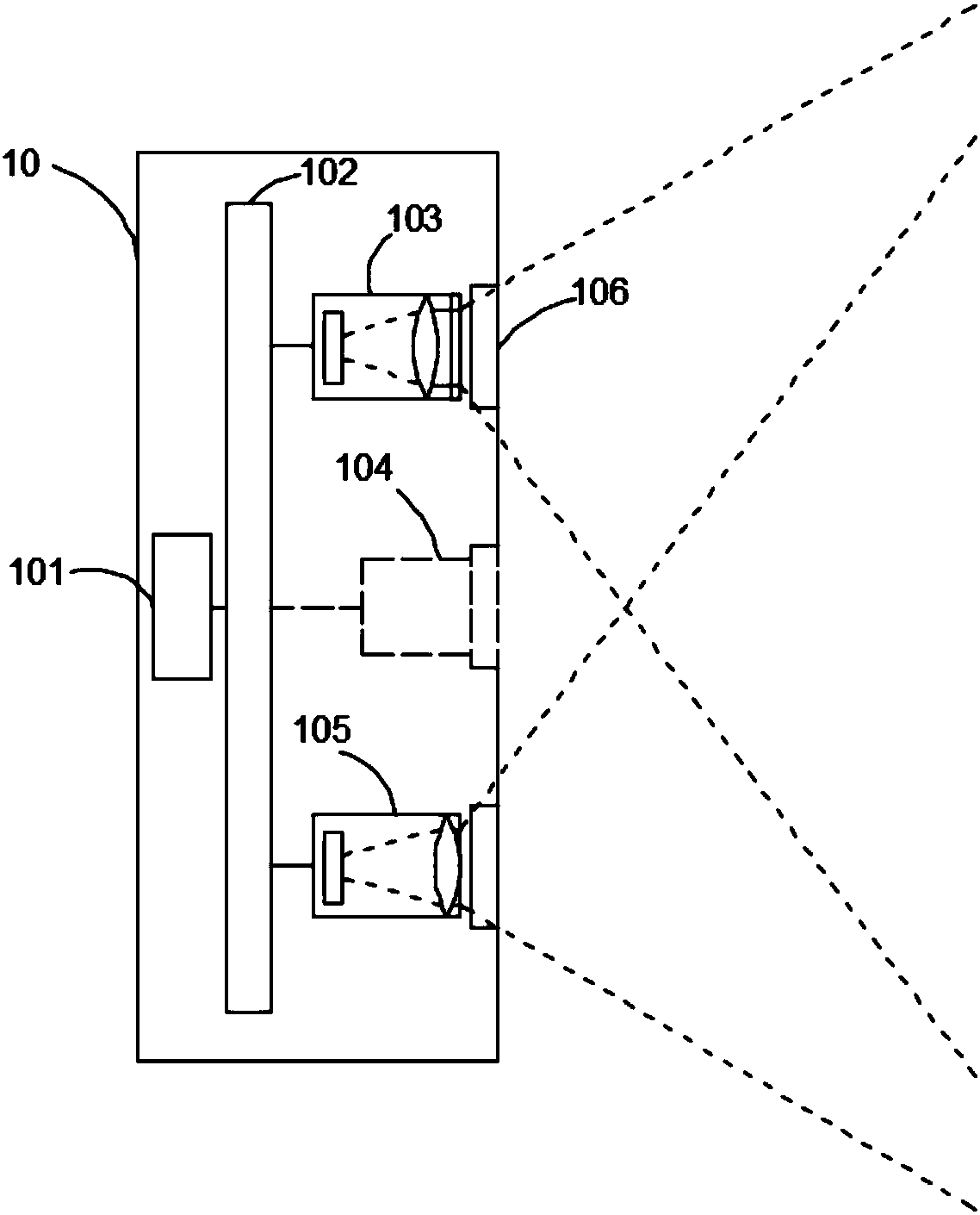
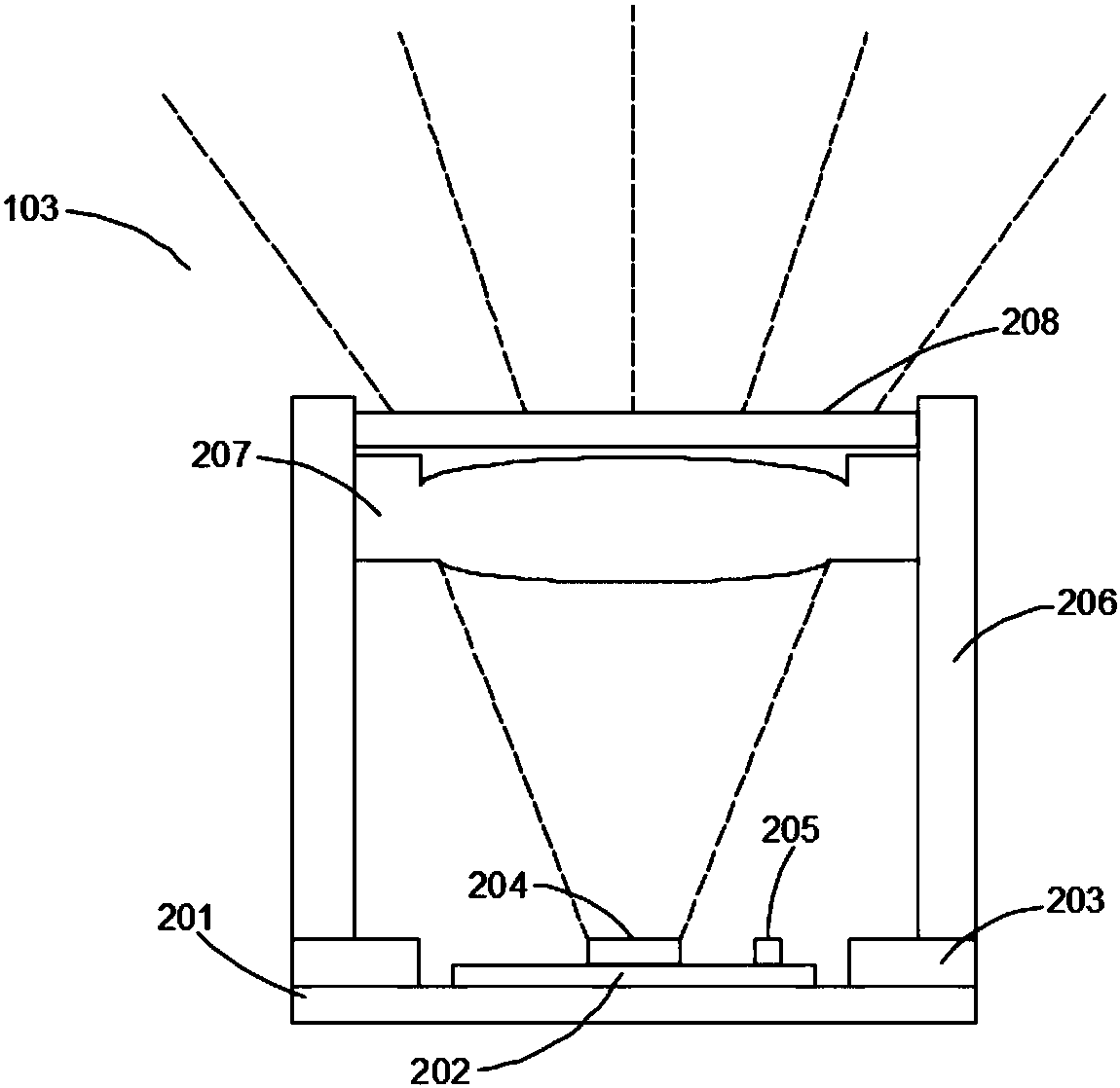
[0020] The invention provides a chip embedding device with good heat dissipation performance and small volume. In the following description, the depth camera projection module and the chip embedding device used in it will be described as e...


PUM


Abstract

The invention provides a chip embedding device. The device comprises a main base, a circuit board, a secondary base and a chip; a through hole is formed in the circuit board which is installed on themain base; the secondary base is installed on the main base and placed in the through hole, the chip is installed on the secondary base, the chip and the secondary base have the matched thermal expansion coefficients, and the chip comprises a vertical cavity surface laser transmitter array chip and/or a thermistor. By arranging the main base and the secondary base with the two different thermal expansion coefficients, the chip is directly connected with the secondary base with the thermal expansion coefficient matched with that of the chip, and then the small size and high stability can be achieved; in addition, the base has the heat dissipation property, and then it is guaranteed that the maximum heat dissipation is provided for the chip. Compared with the prior art, the chip embedding device can achieve small size, high stability and high heat dissipation, and then the device can be integrated into a micro computing device.

Description

technical field [0001] The invention relates to the field of manufacturing electronic and optical components, in particular to a chip embedding device, a manufacturing method and a projection module. Background technique [0002] The depth camera can obtain the depth information of the target to realize 3D scanning, scene modeling, and gesture interaction. Compared with the currently widely used RGB camera, the depth camera is gradually being valued by all walks of life. For example, the combination of depth camera, TV, computer, etc. can realize somatosensory games to achieve the effect of two-in-one game and fitness. In addition, Google's tango project is committed to bringing depth cameras to mobile devices, such as tablets and mobile phones, so as to bring a completely subversive experience. For example, it can realize a very real AR game experience, and can use it for indoor map creation and navigation. and other functions. [0003] The core component of the depth cam...

Claims


Application Information

Patent Timeline
Patent Type & Authority Applications(China)
IPC IPC(8): G03B21/20G03B21/16G03B21/14
CPCG03B21/14G03B21/16G03B21/2033
Inventor 黄杰凡周宇
Owner SHENZHEN ORBBEC CO LTD
Why Eureka
Try Eureka