Display panel and production method thereof as well as display device

A technology of a display panel and a manufacturing method, applied in the fields of display devices and display panels, can solve problems such as affecting the touch effect, and achieve the effects of avoiding touch blind areas, reducing resistivity, and reducing the length of traces

Active Publication Date: 2018-06-29
BOE TECH GRP CO LTD
View PDF4 Cites 2 Cited by
  • Summary
  • Abstract
  • Description
  • Claims
  • Application Information

AI Technical Summary

Problems solved by technology

The OLED In cell touch solution uses the same layer of wiring. When the size of the display panel increases, the touch blind area formed by the wiring area will be too large, which will affect the touch effect.

Method used


Image

  • Display panel and production method thereof as well as display device
  • Display panel and production method thereof as well as display device
  • Display panel and production method thereof as well as display device

Examples


Embodiment Construction

[0036] The present invention will be further described below with reference to the accompanying drawings and exemplary embodiments, wherein the same reference numerals in the accompanying drawings all refer to the same components. Also, detailed descriptions of known arts will be omitted if they are unnecessary to illustrate the features of the present invention.

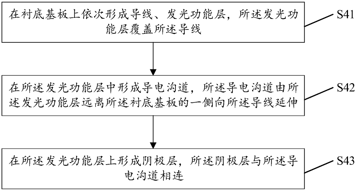
[0037] The present invention provides a method for manufacturing a display panel, the flow chart of which is shown in Figure 3, and the specific steps are as follows:

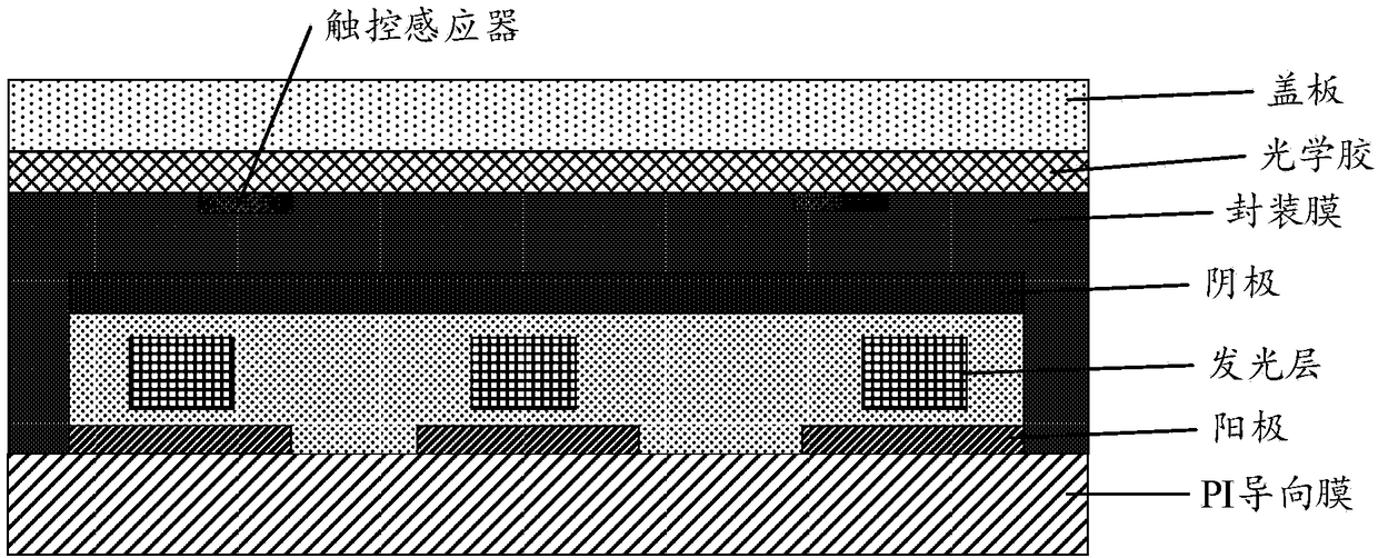
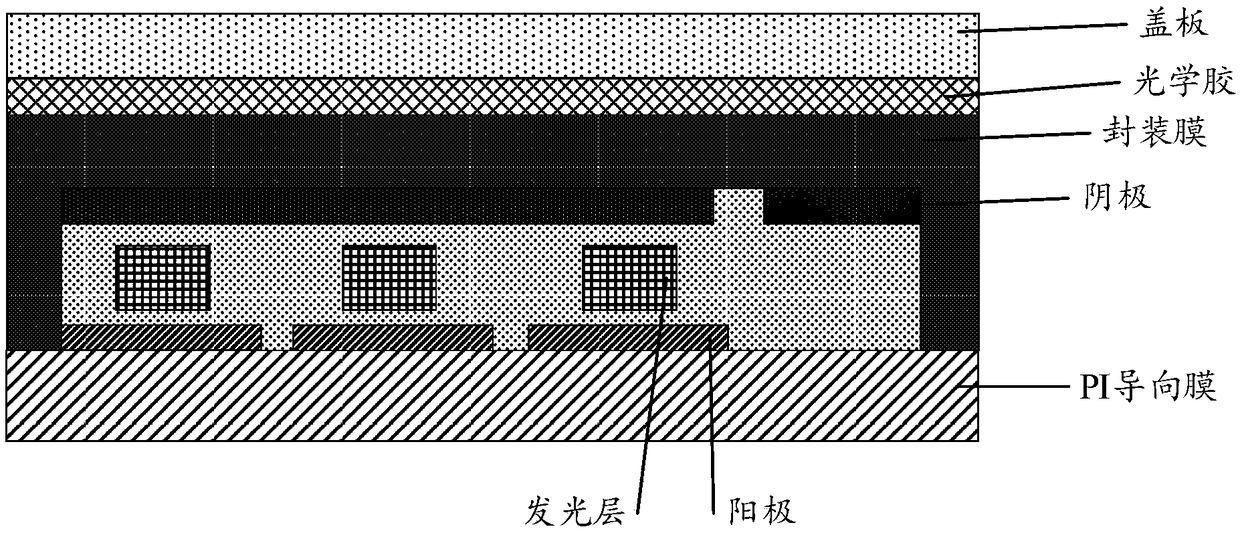
[0038] S41, sequentially forming a wire and a light-emitting functional layer on the base substrate, the light-emitting functional layer covering the wire.

[0039] Specifically, wires can be formed by evaporation, sputtering, or inkjet printing, and the material of the wires is preferably metal, that is, metal wires; the luminescent functional layer is deposited on the substrate by sputtering, evaporation, etc. On, make the light-emitting functiona...


PUM


Abstract

The invention relates to the technical field of display and particularly relates to a display panel and a production method thereof. The production method of the display panel comprises the followingsteps: successively forming lead wires and a light-emitting function layer on a substrate, wherein the light-emitting function layer covers the lead wires; forming conducting channels in the light-emitting function layer, wherein the conducting channels extend from one side away from the substrate of the light-emitting function layer to the lead wires; forming a cathode layer on the light-emittingfunction layer, wherein the cathode layer is connected with the conducting channels. According to the scheme, conducting particles are poured into the light-emitting function layer to form the conducting channels, so that the cathode is connected with the lead wires; the wiring length between the cathode and the lead wires is reduced; the touch control blind area on the display panel caused by the oversized wiring area is avoided.

Description

【Technical field】 [0001] The invention relates to the field of display technology, in particular to a display panel, a manufacturing method thereof, and a display device. 【Background technique】 [0002] With the rapid development of display technology, Organic Light Emitting Diode (OLED) has become the next generation of display due to its fast response, higher contrast, wide viewing angle, ultra-thin, low power consumption, and flexibility. The best choice for the screen. At present, the commonly used touch method for OLED products is on-cell embedded touch technology. The structure diagram of the OLED panel using this touch technology is as follows: figure 1 As shown, the touch sensing layer is prepared on the TFE packaging film, which reduces the number of touch sensing panels, the screen becomes thinner, the touch is more sensitive, and the color rendering is brighter. However, this solution cannot realize the integration of touch and display driver chips. integrated. ...

Claims


Application Information

Patent Timeline
Patent Type & Authority Applications(China)
IPC IPC(8): H01L21/77H01L27/32
CPCH01L21/77H10K59/40H10K59/131G06F3/0412G06F2203/04103H10K50/82H10K59/1201
Inventor 陈亮王磊陈小川玄明花杨盛际刘冬妮岳晗杨明肖丽卢鹏程
Owner BOE TECH GRP CO LTD
Why Eureka
Try Eureka