Gate scan drive circuit

A driving circuit and gate scanning technology, applied in static indicators, instruments, etc., can solve the problems of weak maintenance capability of the driving circuit unit, wrong opening of the scanning signal Gn, affecting the pull-up control node, etc., to save layout space and improve the performance. Circuit reliability, the effect of preventing the narrowing of the signal pulse width

Active Publication Date: 2020-08-04
NANJING CEC PANDA LCD TECH
View PDF7 Cites 0 Cited by
  • Summary
  • Abstract
  • Description
  • Claims
  • Application Information

AI Technical Summary

Problems solved by technology

This phenomenon will affect the function of the pull-up control node maintenance module 4, resulting in a weak maintenance capability of the drive circuit unit after outputting the scan signal Gn, which may cause the scan signal Gn to be turned on by mistake, resulting in poor circuit reliability

Method used


Image

  • Gate scan drive circuit
  • Gate scan drive circuit
  • Gate scan drive circuit

Examples


Embodiment 1

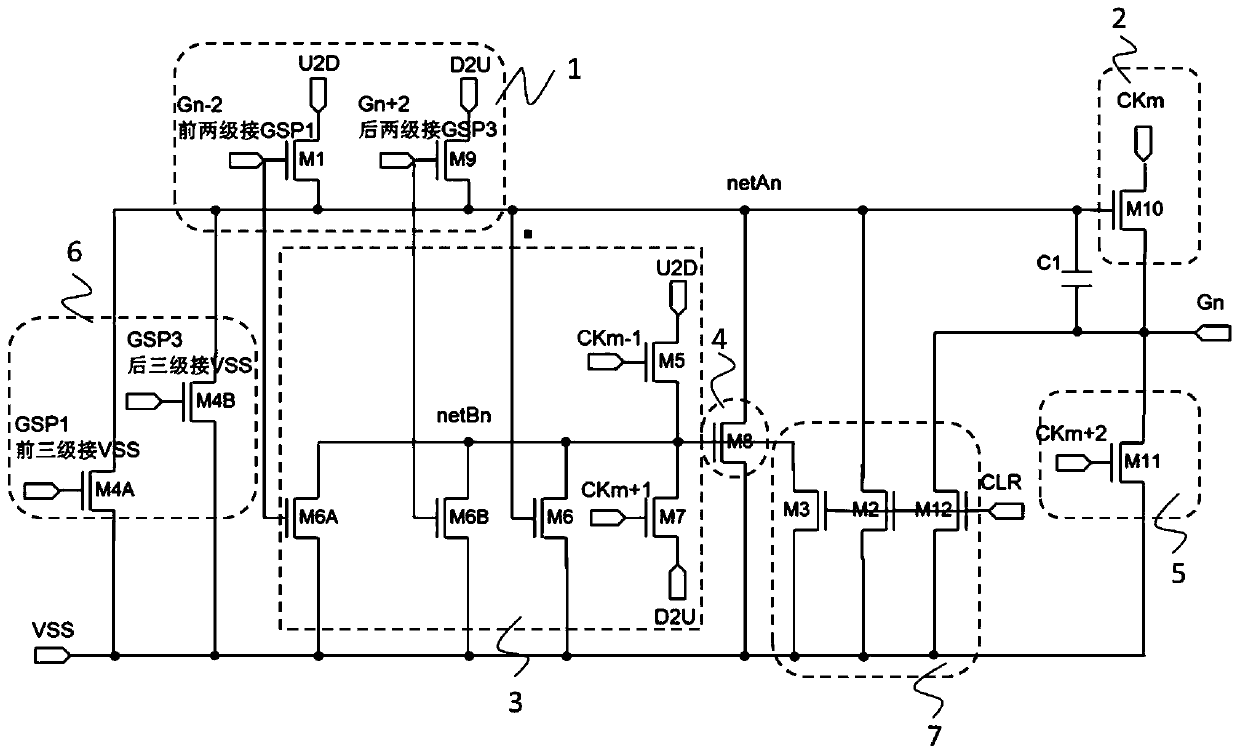
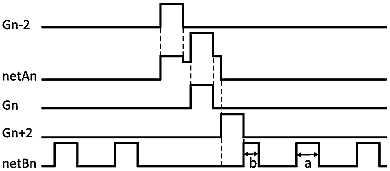
[0062] Such as Figure 6 Shown is a circuit diagram of Embodiment 1 of a gate scanning drive circuit. The nth level drive circuit unit includes a pull-up control module 1, a pull-up module 2, a maintenance control node generation module 3, a pull-up control node maintenance module 4, The output node maintains the module 5 and the bootstrap capacitor C1.

[0063]The pull-up control module 1, the pull-up module 2, the maintenance control node generation module 3 and the pull-up control node maintenance module 4 are connected to the pull-up control node netAn; the maintenance control node generation module 3, the pull-up control node maintenance module 4 and the output The node maintenance modules 5 all input low-level VSS; the pull-up module 2 and the output node maintenance module 5 are connected to the scanning signal line of the current stage, and the scanning signal line outputs the scanning signal Gn; the maintenance control node generation module 3 and the pull-up control ...

Embodiment 2

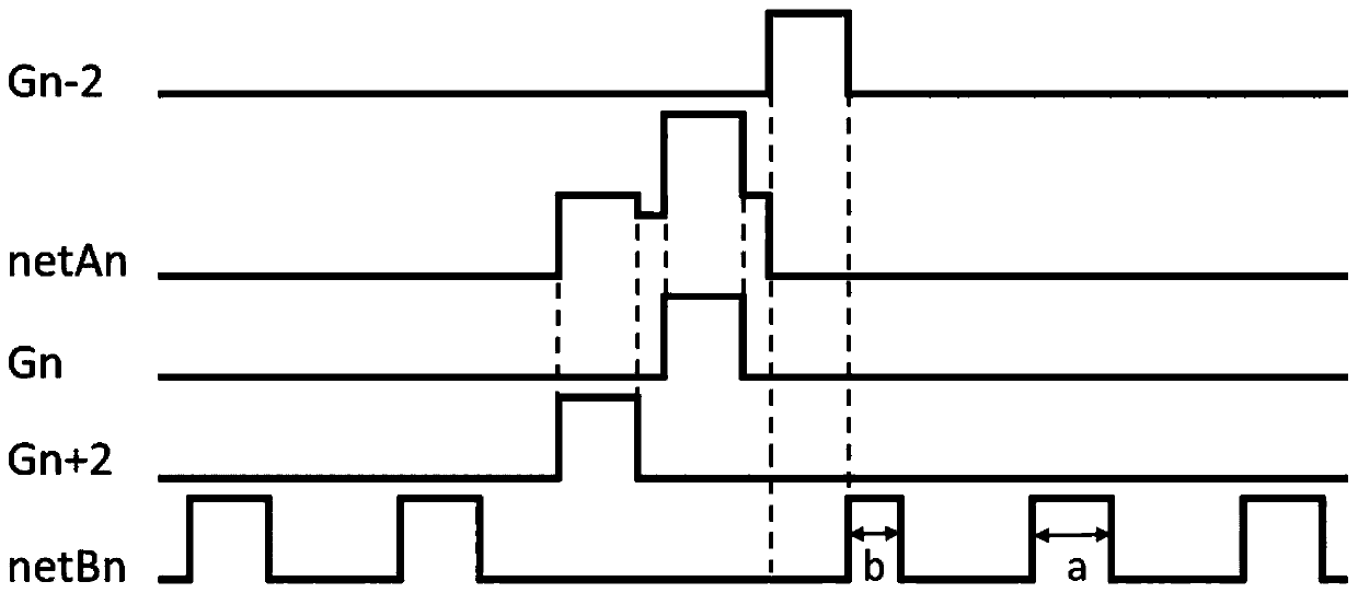
[0108] Figure 9 It is a schematic circuit diagram of Embodiment 2 of a gate scanning driving circuit of the present invention. The second embodiment is improved on the basis of the first embodiment, and the specific improvements are as follows:

[0109] The sustain control node generation module 3 further includes a fourteenth thin film transistor M6A and a fifteenth thin film transistor M6B.

[0110] The control terminal of the fourteenth thin film transistor M6A inputs the first control signal, and the two pass terminals of the fourteenth thin film transistor M6A are respectively connected to the sustain control node netBn of the nth driver circuit unit and the reverse scan control signal D2U. The fourteenth thin film transistor M6A is used to prohibit and maintain the output of the control node netBn during the working period of the n-2th stage circuit unit in the forward scan process, that is, during the precharge phase of the forward scan.

[0111] The control terminal...


PUM


Abstract

A gate drive unit circuit, a gate drive circuit and a liquid crystal display apparatus. The gate drive unit circuit comprises a pull-up control module (1), a pull-up module (2), a holding control node generation module (3), a pull-up control node holding module (4) and an output node holding module (5), wherein the holding control node generation module (3) is used for generating, under the control of a forward scanning control signal (U2D) and a reverse scanning control signal (D2U), that are opposite each other in phase, a holding control signal to control a holding control node (netBn) of the current stage, so that after scanning signals are output during forward scanning and reverse scanning, the first signal pulse width of the holding control node (netBn) of the present stage is the same as the pre-set width. The first pulse width of a holding control node (netBn) can be prevented from being reduced, such that the pull-up control node holding module (4) can immediately carry out intermittent low-potential holding on a pull-up control node (netAn), thus improving the reliability of a circuit.

Description

technical field [0001] The invention relates to the field of liquid crystal display, in particular to a grid scanning driving circuit. Background technique [0002] The gate scanning lines of flat panel displays were generally driven by integrated circuit chips (Gate IC) before, and the integrated gate scanning drive circuit (Gate Driver Monolithic, GDM) is a method that utilizes the existing manufacturing process of thin film transistor array substrates. The technology in which the gate scanning driving circuit is directly built on the array substrate has the functions of reducing cost, reducing process flow, and reducing the width of the panel frame. With the development of products and technologies, flat panel displays have higher and higher requirements for gate scanning driving circuits, one of which is to have forward scanning and reverse scanning functions at the same time. [0003] Such as figure 1 As shown, it is a schematic circuit diagram of an existing bidirect...

Claims


Application Information

Patent Timeline
Patent Type & Authority Patents(China)
IPC IPC(8): G09G3/36
CPCG09G3/3674G09G3/20G09G3/3677G09G2310/0267G09G2310/0286
Inventor 戴超夏迪黄洪涛
Owner NANJING CEC PANDA LCD TECH
Why Eureka
Try Eureka