Display backplane and manufacturing method thereof, display panel and display device

A technology for displaying backplanes and substrates, which is applied to electrical components, electric solid-state devices, circuits, etc., and can solve problems such as the structural design of array substrates needs to be improved, it is difficult to realize, and the light-emitting area is reduced.

A technology for displaying backplanes and substrates, which is applied to electrical components, electric solid-state devices, circuits, etc., and can solve problems such as the structural design of array substrates needs to be improved, it is difficult to realize, and the light-emitting area is reduced.

CN108257977AActive Publication Date: 2018-07-06BOE TECH GRP CO LTD

Image

  • Display backplane and manufacturing method thereof, display panel and display device
  • Display backplane and manufacturing method thereof, display panel and display device
  • Display backplane and manufacturing method thereof, display panel and display device

Examples


Embodiment Construction

[0086] The following describes the embodiments of the present invention in detail, and those skilled in the art will understand that the following embodiments are intended to explain the present invention, and should not be regarded as limiting the present invention. Unless otherwise specified, in the following examples that do not explicitly describe specific techniques or conditions, those skilled in the art can carry out according to commonly used techniques or conditions in this field or according to product instructions.

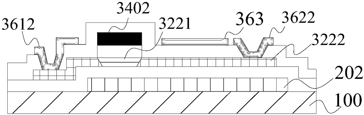
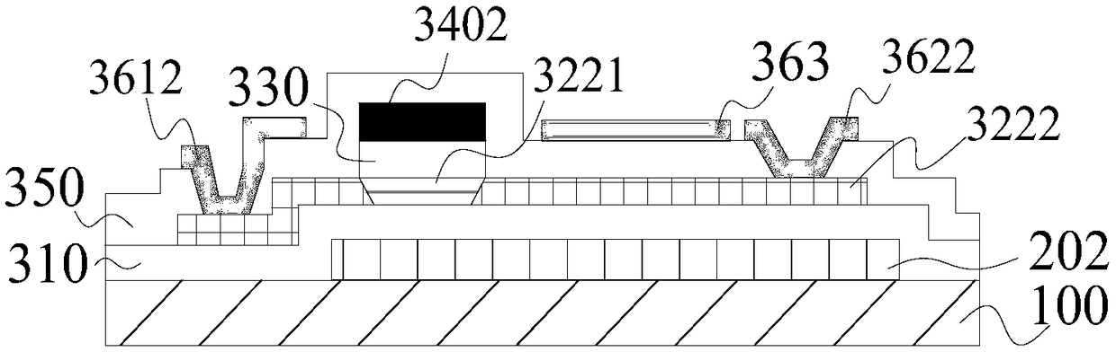
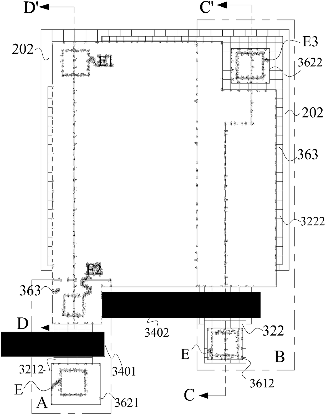
[0087] In one aspect of the invention, the invention provides a display backplane. refer to Figure 1~5 , 8-19, the display backplane of the present invention is described in detail. It should be noted that in this paper, Figure 1~2 The shown structural diagram of the display backplane is a schematic diagram of the cross-sectional structure along the direction of the driving TFT (DR tube) from the drain (D) to the source (S), and image 3 , 8 11, 1...


PUM


Abstract

The invention provides a display backplane and a manufacturing method thereof, a display panel and a display device. The display backplane comprises a substrate, a first shading layer, a first thin film transistor, a first film layer and a third electrode. The first shading layer is arranged on one side of the substrate. The first thin film transistor is arranged on one side of the first shading layer away from the substrate, and includes a first active layer, a first source, a first drain and a first top gate electrode. The first film layer includes a first semiconductor part and a first conductor part, and the first semiconductor part constitutes the first active layer. The third electrode is arranged in the same layer as the first drain. The first shading layer and the first conductor part constitute a first capacitor. The third electrode and the first conductor part constitute a second capacitor. The shading layer of the display backplane not only can protect the light stability ofthe TFT structure from influence, but also can constitute a laminated pixel capacitor together with the first conductor part and the third electrode. The laminated capacitor structure can achieve high opening rate and high PPI while increasing the pixel capacitance value and improving the driving performance.

Description

technical field [0001] The present invention relates to the field of display technology, in particular, the present invention relates to a display backplane and a manufacturing method thereof, a display panel and a display device. Background technique [0002] At present, in order to improve the light-shielding effect of the top-gate thin film transistor (TFT), it is necessary to deposit a layer of metal on the glass as a light-shielding (SH) layer, and in order not to keep the layer of metal in a floating (Floating) state, it is necessary to combine the light-shielding layer with the The source end of the TFT is shorted. Although this connection scheme can meet the requirements of the bottom emission display for the normal I-V characteristics and NBTIS characteristics of the TFT, it does not have the effect of increasing the on-state current compared with the switch (Switch) TFT. [0003] For bottom emission display, it can be designed as active layer (ACT, whose potential...

Claims


Application Information

Patent Timeline
06 Jul 2018
Publication
CN108257977A
IPC
H01L27/12
CPC
H01L27/1218; H01L27/124; H01L27/1262; H01L27/127; H01L27/1255; H01L29/78633; H01L29/78648
Inventors
ๅฎ‹ๆŒฏ; ็Ž‹ๅ›ฝ่‹ฑ