Chip routing method

A wiring method and chip technology, applied in instruments, calculations, electrical digital data processing, etc., can solve problems such as easy congestion and low chip wiring efficiency, and achieve the effect of improving wiring efficiency and eliminating wiring congestion

Active Publication Date: 2021-09-17
HUNAN RONGCHUANG MICROELECTRONICS CO LTD
View PDF7 Cites 0 Cited by
  • Summary
  • Abstract
  • Description
  • Claims
  • Application Information

AI Technical Summary

Problems solved by technology

[0003] The purpose of the embodiments of the present invention is to provide a chip wiring method to solve the problem of low chip wiring efficiency and easy congestion

Method used


Image

  • Chip routing method
  • Chip routing method
  • Chip routing method

Examples


Embodiment Construction

[0039] Exemplary embodiments of the present disclosure will be described in more detail below with reference to the accompanying drawings. While exemplary embodiments of the present disclosure are shown in the drawings, it should be understood that the present disclosure may be embodied in various forms and should not be limited by the embodiments set forth herein. Rather, these embodiments are provided so that the present disclosure will be more thoroughly understood, and will fully convey the scope of the present disclosure to those skilled in the art.

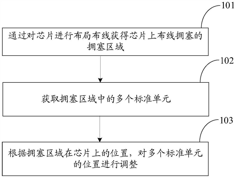
[0040] like figure 1 As shown, a specific embodiment of the present invention provides a chip wiring method, including:

[0041] Step 101 , obtaining a congested area with congested wiring on the chip by performing layout and wiring on the chip.

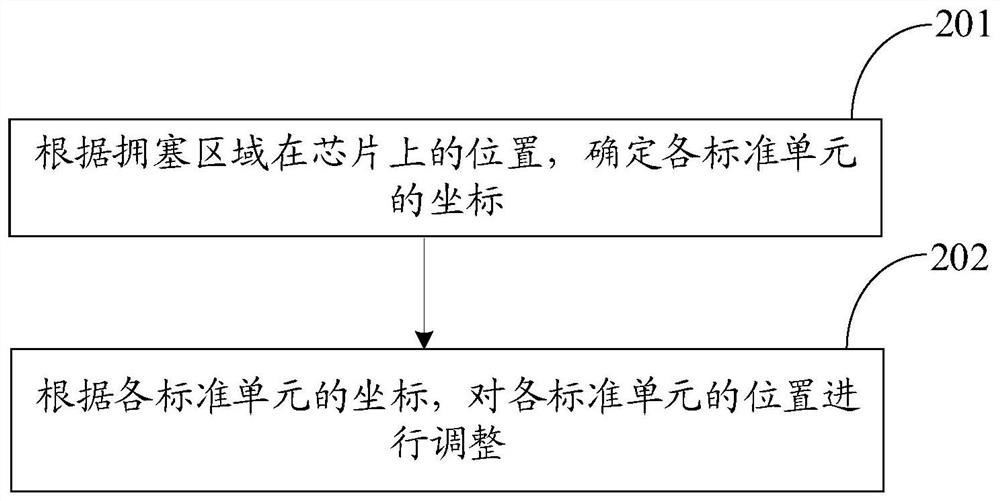
[0042] Wherein, in the specific embodiment of the present invention, the specific implementation manner of the above step 101 may be: performing layout and wiring on the chip by ...


PUM


Abstract

The invention provides a chip wiring method, comprising: obtaining the congested area of ​​wiring congestion on the chip by laying out and wiring the chip; obtaining multiple standard units in the congested area; Adjusting the position of the unit can improve the wiring efficiency of the chip while eliminating wiring congestion.

Description

technical field [0001] The invention relates to the technical field of integrated circuit design, in particular to a chip wiring method. Background technique [0002] In the physical design of integrated circuits, the full utilization of wiring resources can reduce the area of ​​the chip, thereby greatly reducing the cost of the chip and improving the competitiveness of this product in the market. At present, the development of various layout and routing tools is more and more complete, which not only improves the speed of chip design, but also greatly improves the utilization rate of routing resources. However, the placement and routing tools usually take the global chip as the consideration, and it is inevitable that some small points are not considered carefully, and some local congestion will occur during the actual placement and routing process, for example, the area close to the pins of the macrocell (block) (pin) and areas near the corners of the block, etc. At this...

Claims


Application Information

Patent Timeline
Patent Type & Authority Patents(China)
IPC IPC(8): G06F30/392
CPCG06F30/392
Inventor 吴传禄徐庆光杨国庆刘祥远刘浩陈强徐欢杨柳江秦鹏举
Owner HUNAN RONGCHUANG MICROELECTRONICS CO LTD
Why Eureka
Try Eureka