Two-shot molding process for Micro USB connector
A molding process and connector technology, applied in the field of two-time molding process of MicroUSB connector, can solve the problems of low assembly efficiency, low overall strength of the connector, and high defective product rate
- Summary
- Abstract
- Description
- Claims
- Application Information
AI Technical Summary
Problems solved by technology
Method used
Image
Examples
Embodiment Construction
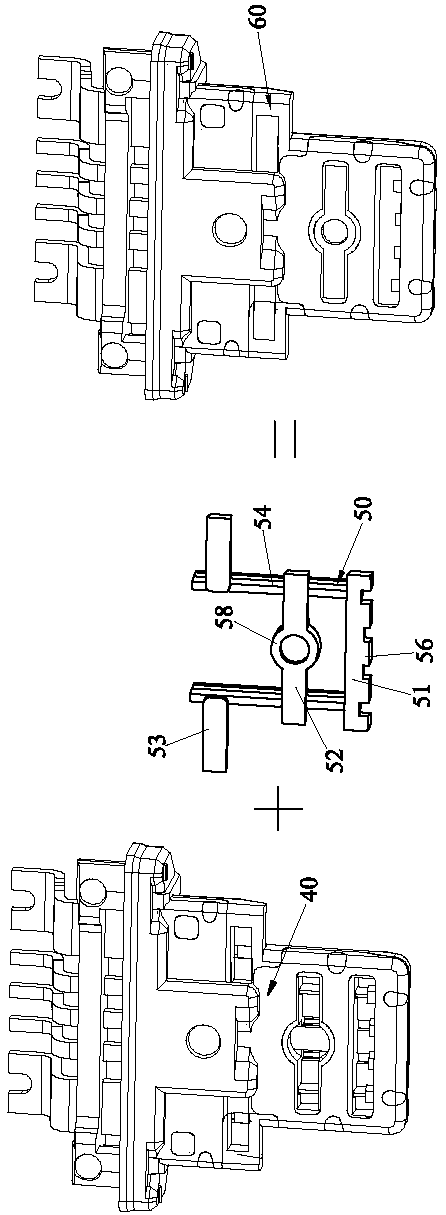
[0049] Please refer to Figure 1 to Figure 6 Shown, it has shown the molding process of preferred embodiment of the present invention, comprises the following steps:
[0050] Step 1: Put the metal frame 20 and a plurality of conductive terminals 10 into the first molding position of the injection mold for positioning. The injection mold has a male mold and a female mold. The mold is formed with multiple terminal positioning parts by digging out glue;
[0051] Step 2: The female mold and the male mold are molded together, and the first injection molding is performed to form the insulating body 30. A plurality of terminal positioning parts are embedded in the insulating body 30, and a plurality of conductive terminals 10 are embedded in the lower surface of the insulating body 30. The metal frame 20 is inlaid on the upper surface of the insulating body 30, and a plurality of conductive terminals 10, the metal frame 20 and the insulating body 30 are embedded and fixed together t...
PUM
 Abstract
Description
Claims
Application Information


