High-multilayer circuit board and manufacturing method thereof

A manufacturing method and circuit board technology, applied in multilayer circuit manufacturing, circuit substrate materials, printed circuit manufacturing, etc., can solve problems such as bubble residue, resin voids, interlayer reliability test failure, etc., to improve the amount of glue filling, Effect of improving heat resistance and insulation, and solving misalignment between laminated layers

Active Publication Date: 2018-07-24
江西景旺精密电路有限公司
View PDF4 Cites 4 Cited by
  • Summary
  • Abstract
  • Description
  • Claims
  • Application Information

AI Technical Summary

Problems solved by technology

[0004] The technical problem to be solved by the present invention is: the interlayer insulation layer of the high-layer circuit board in the prior art is thin

Method used


Image

  • High-multilayer circuit board and manufacturing method thereof
  • High-multilayer circuit board and manufacturing method thereof
  • High-multilayer circuit board and manufacturing method thereof

Examples


Embodiment Construction

[0021] In order to describe the technical content, structural features, achieved goals and effects of the present invention in detail, the following will be described in detail in conjunction with the embodiments and accompanying drawings.

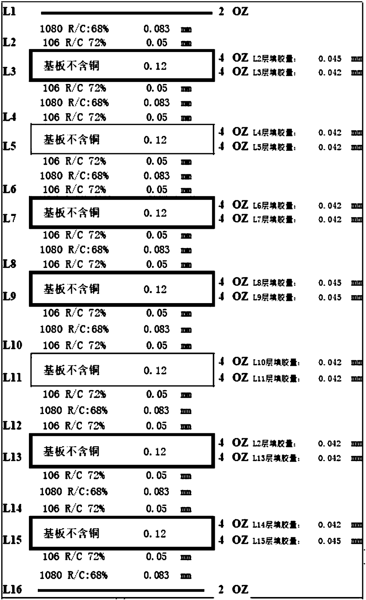
[0022] combine figure 1 , this program designs a high-level circuit board including 16 layers of circuits. The high-level circuit board includes two outer layers of copper foil and seven inner layers of substrates. The upper and lower surfaces of each inner layer substrate are covered with inner layers of copper foil circuits. And the thickness of the outer copper foil is 70um (2 oz / ft 2 ), the copper foil thickness of the inner substrate is 137.2um (4 oz / ft 2 ), the inner substrate is an epoxy resin substrate, and the thickness of the resin is 0.12mm (without copper). At the same time, there are 106 prepregs, 1080 prepregs and 106 prepregs in sequence between any two adjacent inner substrates (L3 layer to L15 layer), and between the out...


PUM

PropertyMeasurementUnit
Thicknessaaaaaaaaaa
Thicknessaaaaaaaaaa

Abstract

The invention provides a high-multilayer circuit board and a manufacturing method thereof, and belongs to the technical field of a circuit board. In the scheme, 106 prepregs and 1080 prepregs are utilized to realize interlayer prepreg combined design, and the high-multilayer circuit board formed like such has a special laminated composite structure with high resin content, thereby improving interlayer glue filling amount, enabling the resin to be able to fully flow and cured, improving heat resistance and insulation of the high-multilayer circuit board and effectively solving the problems of interlayer mismatch (board slip), delamination, resin cavity and bubble residual and the like in the laminating process.

Description

technical field [0001] The invention relates to the technical field of circuit boards, in particular to a high-layer circuit board and a manufacturing method thereof. Background technique [0002] High-layer circuit boards are generally defined as (10-20 layers) or more multi-layer circuit boards, which are more difficult to process than traditional multi-layer circuit boards, and require high quality and reliability. In recent years, the market demand for high-layer boards in the fields of communication, base stations, aviation, and military is still strong. With the continuous development of the electronic information industry, the requirements of electronic products on the signal transmission capacity, frequency and signal fidelity carried by PCB (printed circuit board) are also increasing. Can not meet the market demand. On the one hand, PCB is developing towards high density, high precision, and high integration, which requires that the design layers of PCB products b...

Claims


Application Information

Patent Timeline
IPC IPC(8): H05K1/03H05K3/46
CPCH05K1/036H05K3/4626H05K2201/0195
Inventor 胡定益管术春柯勇周锋
Owner 江西景旺精密电路有限公司
Why Eureka
Try Eureka