A method for suppressing the formation of positive charges captured by oxides in electronic components

A technology of electronic components and oxides, which is applied in the direction of electrical components, semiconductor/solid-state device manufacturing, circuits, etc., can solve the problems of changing the carrier surface recombination rate and affecting the minority carrier lifetime, and achieves cost reduction, easy operation, and wide application The effect of applying the foreground

Active Publication Date: 2020-06-09
HARBIN INST OF TECH
View PDF4 Cites 0 Cited by
  • Summary
  • Abstract
  • Description
  • Claims
  • Application Information

AI Technical Summary

Problems solved by technology

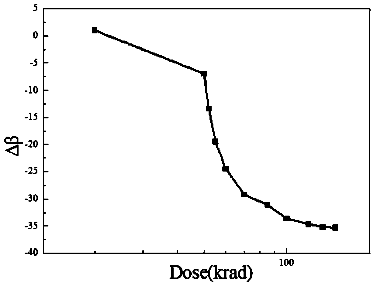
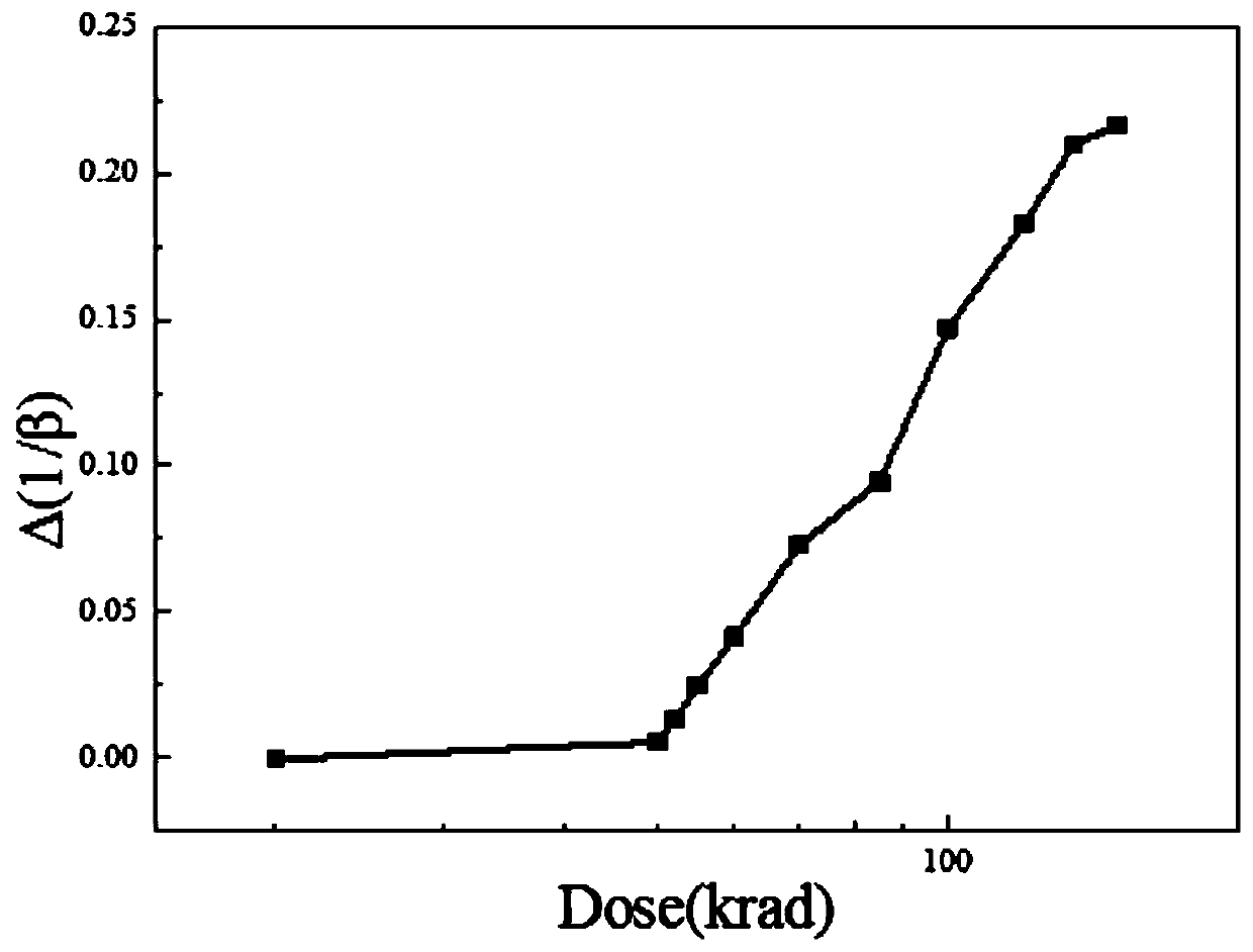
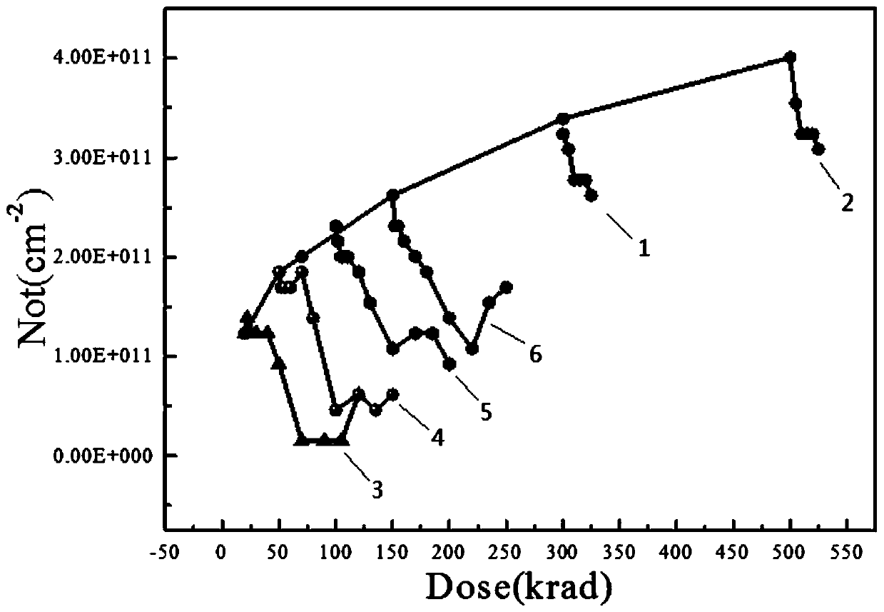
[0004] The present invention is to solve existing SiO 2 Electronic components used as insulating materials and passivation layers have the phenomenon of oxide trapping charge, which changes the surface recombination rate of carriers, thereby affecting the lifetime of minority carriers. It provides a method for inhibiting the capture of positive charges in oxides in bipolar process electronic components. method of formation

Method used


Image

  • A method for suppressing the formation of positive charges captured by oxides in electronic components
  • A method for suppressing the formation of positive charges captured by oxides in electronic components
  • A method for suppressing the formation of positive charges captured by oxides in electronic components

Examples


specific Embodiment approach 1

[0030] Specific implementation mode 1: The method for suppressing the formation of positive charges captured by oxides in bipolar process electronic components in this implementation mode includes the following steps:

[0031] Step 1, determining the chip thickness a of the electronic component sample;

[0032] Step 2: Select the incident particle, input the radiation source energy of the incident particle through Geant4 software, calculate the incident depth d of the incident particle in the sample chip, and ensure that the input radiation source energy satisfies d>4a;

[0033] Step 3, according to the radiation source energy of step 2, by Geant4 software, calculate the ionized absorbed dose (I) of the incident particles of the unit fluence in the sample d ) and displacement absorbed dose (D d );

[0034] According to ionizing absorbed dose (I d ) and displacement absorbed dose (D d ) With the distribution of incident depth, the ionized absorbed dose (I d ) and displacem...

specific Embodiment approach 2

[0041] Specific embodiment 2: The difference between this embodiment and specific embodiment 1 is that the electronic components described in step 1 use SiO 2 Bipolar process electronic components as insulating material and passivation layer. Others are the same as in the first embodiment.

specific Embodiment approach 3

[0042] Embodiment 3: The difference between this embodiment and Embodiment 1 or 2 is that the incident particles in step 2 are photons, mesons, charged particles or neutrons. Others are the same as in the first or second embodiment.


PUM


Abstract

The invention relates to a method for suppressing an oxide in a bipolar process electronic component from capturing positive charge formation. By the method, the problem that charges are captured by the oxide in an existing bipolar process electronic component due to radiation to change carrier surface recombination rate and further affect minority carrier lifetime is solved. The method comprisesthe steps of 1, determining a chip thickness a of a sample; 2, calculating an incident depth d of incident particles in the sample chip; 3, calculating ionization absorption dosage Id and displacementabsorption dosage Dd; 4, allowing log[(Id+Dd) / Dd]; 5, adjusting irradiation flux or dosage rate of the incident particles; 6, performing primary irradiation sample; and 7, performing secondary irradiation and completing. By the method of changing the irradiation flux or the dosage rate, the problem of capturing the positive charges by the oxide in an electronic device is prevented, and the methodis used for suppressing the oxide in the electronic component from capturing the positive charges.

Description

technical field [0001] The invention relates to a method for suppressing the formation of positive charges captured by oxides of electronic components. Background technique [0002] With the development of science and technology, my country's aerospace industry has made great progress and has become one of the aerospace powers. All kinds of spacecraft are closely related to our life and safety. Electronic components used in spacecraft will inevitably be affected by the space environment during their in-orbit service. These factors include solar cosmic ray particles, galactic cosmic ray particles, and radiation environments such as the Earth's radiation belts. Electronic components play a vital role in the electronic control system and information system of a spacecraft. Various radiation environments in space will lead to its performance degradation, abnormal function and even failure. [0003] Space charged radiation particles mainly include electrons, protons and ionized...

Claims


Application Information

Patent Timeline
Patent Type & Authority Patents(China)
IPC IPC(8): H01L21/67
CPCH01L21/67253
Inventor 李兴冀杨剑群刘超铭吕钢
Owner HARBIN INST OF TECH
Why Eureka
Try Eureka