A small outline integrated circuit packaging device

A technology for integrated circuits and packaging devices, which is applied in the field of small-outline integrated circuit packaging devices, can solve problems such as low work efficiency, packaging misalignment, unfavorable packaging production operations, etc., and achieve the effect of improving sealing

Active Publication Date: 2019-12-03
深圳市杰盛微半导体有限公司
View PDF3 Cites 0 Cited by
  • Summary
  • Abstract
  • Description
  • Claims
  • Application Information

AI Technical Summary

Problems solved by technology

[0004] In view of the deficiencies in the prior art, the purpose of the present invention is to provide a small-outline integrated circuit packaging device to solve the problem of low work efficiency caused by the single transfer package in the prior art, which is not conducive to the large-demand packaging production operations, and the packaging process The misalignment of the package caused by it makes the problem of high frequency of defective products

Method used


Image

  • A small outline integrated circuit packaging device
  • A small outline integrated circuit packaging device
  • A small outline integrated circuit packaging device

Examples


Embodiment 1

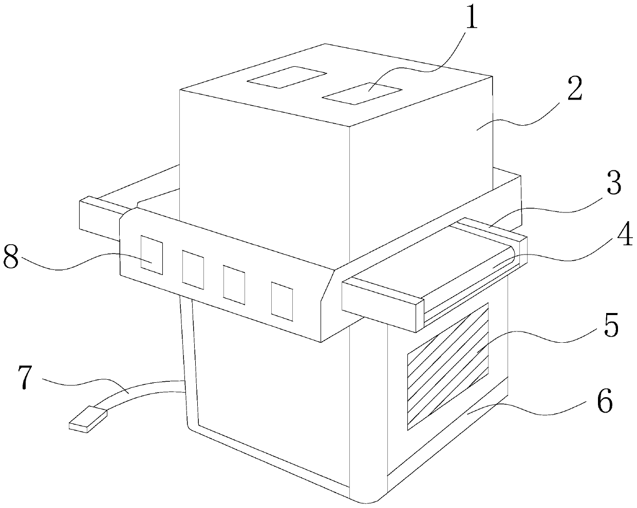
[0030] see Figure 1-Figure 7, the present invention provides a small-outline integrated circuit packaging device, the structure of which includes a substrate inlet 1, a packaging control box 2, a conveyor belt fixing plate 3, a conveyor belt 4, a heat dissipation port 5, a protection base 6, a cable 7, and a control button 8. The upper port of the packaging control box 2 is provided with two substrate inlets 1 for installing the substrate, and the control button 8 is provided with more than two left end half places of the packaging control box 2, and the conveyor belt The inner two ends of the fixed plate 3 are mechanically connected with the conveyor belt 4 and run through the package control box 2. The bottom front end of the package control box 2 is provided with a heat dissipation port 5, and the protective base 6 is welded to the bottom of the package control box 2 and As an integrated structure, the end of the cable 7 runs through the packaging control box 2 and is elec...


PUM


Abstract

The invention discloses a small outline integrated circuit packaging device; the structure comprises a substrate inlet, a packaging control box, a convey belt fixed plate, a conveyer belt, radiating holes, a protection pedestal, a cable wire, and a control button; the packaging control box comprises elevation packaging mechanisms, a power device, a control room, a trigger mechanism, a transmissionmechanism, a lever structure, a first transmission mechanism, a second transmission mechanism, a rotary motor, a driver belt, an energy supply motor and a packaging fixed device. The packaging fixeddevice is arranged in the control room; when a to-be-packaged chip is conveyed to the position via the conveyer belt, the chip weights and triggers chip induction seats; the two chip induction seats are matched with the elevation packaging mechanisms one by one; only when the to-be-packaged chip is conveyed to the chip induction seats, the packaging work can be started, thus preventing packaging offset; the dual packaging mechanisms and chip induction seats can effectively improve the packaging efficiency, and can reduce the defective product forming rates.

Description

technical field [0001] The invention is a small-outline integrated circuit packaging device, which belongs to the field of integrated circuit packaging devices. Background technique [0002] An integrated circuit is a microelectronic device or component that uses a certain process to interconnect components such as transistors, resistors, capacitors, and inductors required in a circuit, and interconnects them together to form a small or several small semiconductor chips or chips. Dielectric substrate, and then packaged in a package, to become a microstructure with the required circuit functions; all the components have been integrated in the structure, making electronic components towards miniaturization, low power consumption, intelligence and high reliability. A big step forward in terms of performance, it is represented by the letters "IC" in the circuit. It is a new type of semiconductor device developed in the late 1950s and 1960s. It is a semiconductor manufacturing ...

Claims


Application Information

Patent Timeline
Patent Type & Authority Patents(China)
IPC IPC(8): H01L21/56H01L21/67H01L21/677
CPCH01L21/56H01L21/67121H01L21/67259H01L21/67742
Inventor 梁瑞城
Owner 深圳市杰盛微半导体有限公司
Why Eureka
Try Eureka