Camera module packing method

A camera module and packaging technology, which is applied in the field of cameras, can solve problems such as irreparable, glue overflow, chip photosensitive area failure, etc., and achieve the effect of avoiding plastic overflow

Active Publication Date: 2018-08-17
JIANGXI HOLITECH TECH
View PDF1 Cites 3 Cited by
  • Summary
  • Abstract
  • Description
  • Claims
  • Application Information

AI Technical Summary

Problems solved by technology

At present, most of the most common packaging processes are based on the MOC packaging process, but in the actual implementation, we must also consider a very likely thing: plastic overflow; Figure 5 , the existing MOC process requires very high mold precision and injection molding precision. If there is a deviation in the mold or during injection molding, it may cause plastic overflow to the photosensitive area of ​​the chip, resulting in damage to the photosensitive chip
If the tolerance control of the mold is not good, or the PCB is deformed, it is easy to overflow the glue
Once the plastic injection overflows to the photosensitive area of ​​the chip, it will cause the failure of the photosensitive area of ​​the chip, and because the photosensitive area of ​​the chip is very fragile, such defects are irreparable

Method used


Image

  • Camera module packing method
  • Camera module packing method
  • Camera module packing method

Examples


Embodiment 1

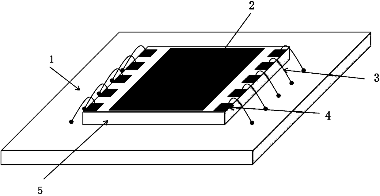
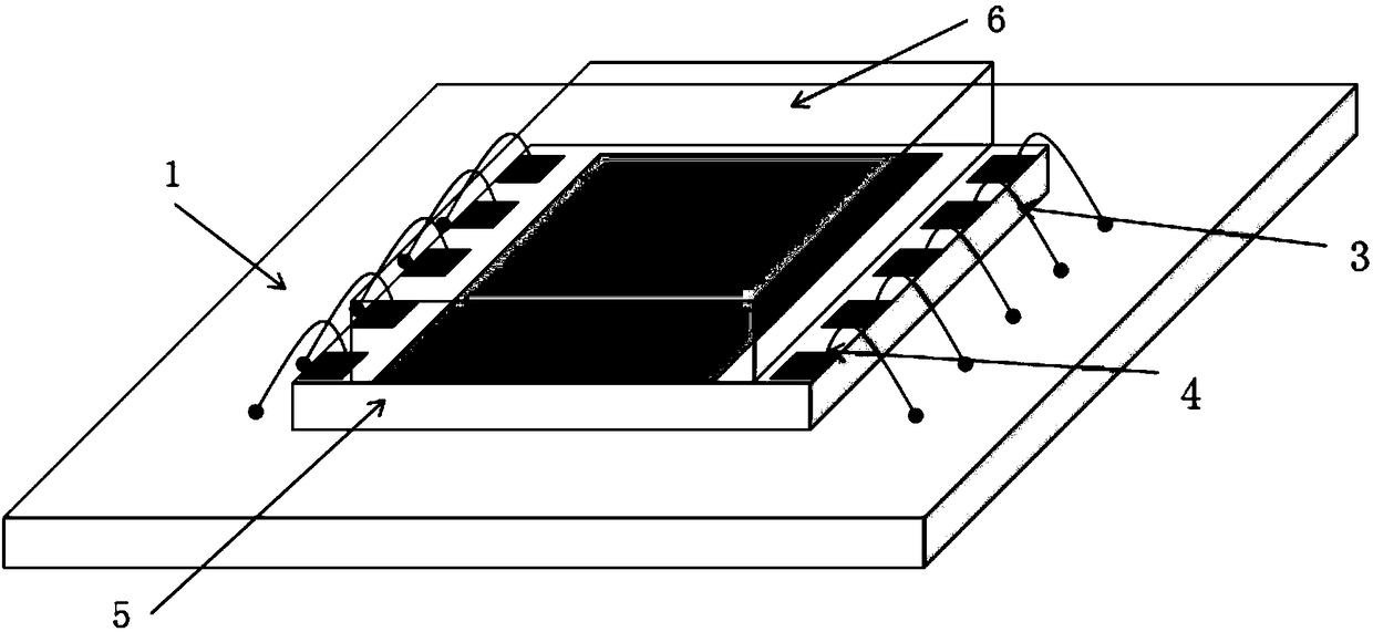
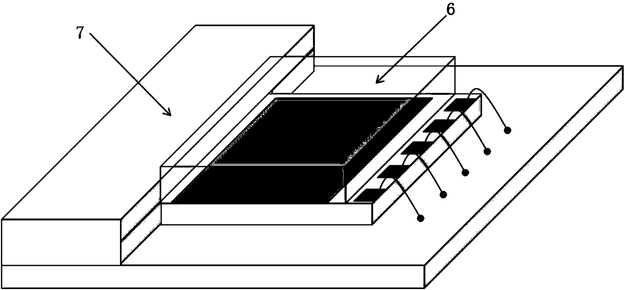
[0021] Embodiment 1: A camera module assembly method, comprising the following steps: Step 1, according to the size of the chip photosensitive area 2 of the photosensitive chip 5 and the distance between the chip photosensitive area 2 and the pad, design a filter of a suitable size 6. The size of the optical filter 6 should not be smaller than the size of the photosensitive area 2 of the chip, and at the same time, it cannot cover the pad 4 of the photosensitive chip; step 2, such as figure 2 , the filter 6 is attached on the chip photosensitive area 2 of the photosensitive chip 5, covering the chip photosensitive area 2 and not covering the photosensitive chip pad 4; Step 3, as figure 1 , the photosensitive chip 5 is bound to the circuit board 1; Step 4, as image 3 , and then place the components after step 2 in the mold for molding, and use the method of plastic sealing molding to inject injection plastic 7 on the circuit board 1 to form a plastic package, which covers th...

Embodiment 2

[0022] Embodiment two: a camera module assembly method, comprising the following steps: step one, such as figure 1 , the photosensitive chip 5 is bound to the circuit board 1; Step 2: as figure 2 According to the chip photosensitive area 2 size of the photosensitive chip 5 and the distance between the chip photosensitive area 2 and the welding pad, the filter 6 of suitable size is designed, and the size of the optical filter 6 is not less than the size of the chip photosensitive area 2, and at the same time Can not cover photosensitive chip pad 4; Step 3, attach filter 6 on chip photosensitive area 2 of photosensitive chip 5, cover chip photosensitive area 2 and do not cover photosensitive chip pad 4; Step 4, as image 3 , placed in the mold used for molding, using the method of plastic sealing molding, injection plastic 7 is injected on the circuit board 1 to form a plastic package, and the plastic package covers the non-photosensitive area of ​​the photosensitive chip 5; S...

Embodiment 3

[0023] Embodiment 3: On the basis of Embodiment 1 or 2, the filter 6 is an ultraviolet filter or a narrow-band filter, and the others are the same.

[0024] Implementation principle: such as Figure 5 , The current camera modules all have infrared cut-off filters inside, and the infrared cut-off filters in the prior art solutions are all bonded on the lens bracket by glue. However, the present invention directly attaches the infrared cut-off filter to the surface of the photosensitive area 2 of the chip, and then performs MOC injection molding, thereby preventing the injection plastic 7 from overflowing into the photosensitive area 2 of the chip, such as Figure 4 .

[0025] Compared with the prior art, the above embodiment has the beneficial effects that: the photosensitive area of ​​the chip is protected by the optical filter, and the injection molding plastic will not overflow to the photosensitive area of ​​the chip, avoiding the problem of plastic overflow.


PUM


Abstract

The invention provides a camera module packing method. Based on a traditional MOC technology, an optical filter is bonded on a light sensing area before an integral injection molding step, and is placed in a mold for molding; injection molding plastic is injected in a circuit board to form a plastic packing body; a non-light sensing area of a light sensing chip is coated by the plastic packing body; and the plastic can be prevented from overflowing to the light sensing area of the chip.

Description

【Technical field】 [0001] The invention relates to the technical field of cameras, in particular to a camera module assembly method. 【Background technique】 [0002] A camera is a widely used electronic device component, commonly used in smartphones, driving recorders, monitors, etc. The camera includes at least a photosensitive element, a circuit board, and an imaging component, and may also include a filter component, an optical focusing component, etc., and all components are packaged together to become a camera component that can be directly applied to electronic equipment. Commonly used packaging methods include COB (Chip on Board), that is, the photosensitive chip is bonded to the substrate through gold wires, and then the lens and bracket (or motor) are bonded to the substrate; CSP (Chip Scale Package), that is, the photosensitive chip is passed through SMT is soldered to the substrate, and then the lens and bracket (or motor) are bonded to the substrate; MOB (Mold on ...

Claims


Application Information

Patent Timeline
Patent Type & Authority Applications(China)
IPC IPC(8): B29C45/14H04N5/225B29L31/34
CPCB29C45/14336B29C45/14639B29C2045/14852B29L2031/3425H04N23/50H04N23/55
Inventor 周晴
Owner JIANGXI HOLITECH TECH
Why Eureka
Try Eureka