Array substrate, preparing method thereof, display panel and display device

A technology for array substrates and display panels, applied in instruments, semiconductor devices, computing, etc., can solve problems such as poor X-line, reduced aperture ratio, and insufficient aperture ratio, and achieve avoidance of x-line defects, high aperture ratio, and aperture ratio high effect

Inactive Publication Date: 2018-08-21
BOE TECH GRP CO LTD +1
View PDF5 Cites 12 Cited by
  • Summary
  • Abstract
  • Description
  • Claims
  • Application Information

AI Technical Summary

Problems solved by technology

[0002] Products with full in-cell touch structure (FIC, Full in Cell), high pixel (PPI), and high aperture ratio are the main development direction of low temperature polysilicon liquid crystal display panel (LTPS LCD). However, with the increase of PPI, The existing Fullin Cell LCD product design will inevitably face the dilemma of insufficient aperture ratio; specifically, in the existing panel design, the data line (Date signal line) and the touch electrode line (TPM signal line) are arranged on the same layer , and the signal line uses Ti / AL / Ti light-shielding material, which leads to a great reduction in the aperture ratio of existing products; at the same time, due to the small distance between the Date signal line and the TPM signal line, it is often due to the remaining material (remain ) or particles cause a short circuit, which leads to the voltage of the Date signal line being pulled down during driving, so that the Data signal line cannot drive the pixels normally, resulting in a bad x-line

Method used


Image

  • Array substrate, preparing method thereof, display panel and display device
  • Array substrate, preparing method thereof, display panel and display device
  • Array substrate, preparing method thereof, display panel and display device

Examples


Embodiment Construction

[0036] The following will clearly and completely describe the technical solutions in the embodiments of the present invention with reference to the accompanying drawings in the embodiments of the present invention. Obviously, the described embodiments are only some, not all, embodiments of the present invention. Based on the embodiments of the present invention, all other embodiments obtained by persons of ordinary skill in the art without making creative efforts belong to the protection scope of the present invention.

[0037] Please refer to Figure 1 to Figure 6 .

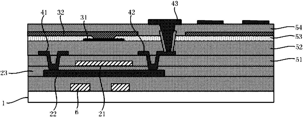
[0038] like figure 1 and figure 2 As shown, an array substrate provided by an embodiment of the present invention includes:

[0039] Substrate 1, a plurality of pixels are arranged in an array in its pixel area;

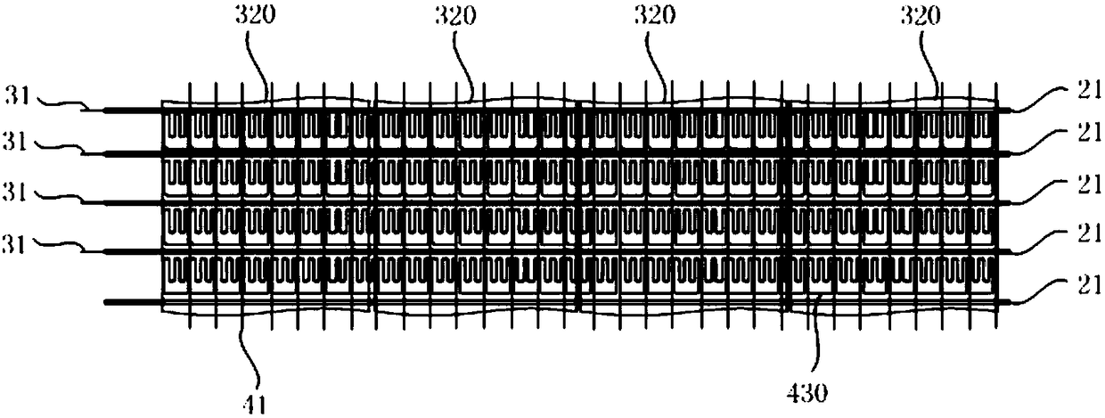
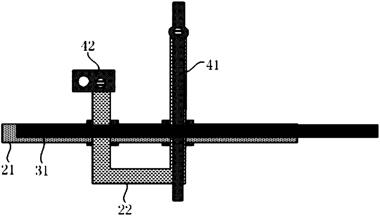
[0040] A plurality of gate lines (Gate lines) 21 are formed on the substrate 1 to extend along the first direction of the pixel array;

[0041] A plurality of touch electrode traces (TPM traces) ...


PUM


Abstract

The invention relates to the technical field of display, and discloses an array substrate, a preparing method thereof, a display panel and a display device. The array substrate comprises a substrate body, a plurality of grid wires and a plurality of touch control electrode wires, wherein a plurality of pixels are arranged in a pixel area of the substrate body in arrays, the grid wires extend on the substrate body in the first direction of the pixel arrays, the touch control electrode wires extend on the substrate body in the first direction of the pixel arrays and are insulated from the grid wires, and the positive projection of the touch control electrode wires on the substrate body and the positive projection of the grid wires on the substrate body are at least partly overlapped. Compared with similar array substrates in the prior art, the array substrate has the advantages that the display area occupied by signals wires is small, the opening rate of the pixels is large, the short-circuit situation between the touch control electrode wires and the data wires cannot easily happen, the opening rate of the array substrate is high, and the x-line failures can be avoided.

Description

technical field [0001] The present invention relates to the field of display technology, in particular to an array substrate and a preparation method thereof, a display panel, and a display device. Background technique [0002] Products with full in-cell touch structure (FIC, Full in Cell), high pixel (PPI), and high aperture ratio are the main development direction of low temperature polysilicon liquid crystal display panel (LTPS LCD). However, with the increase of PPI, The existing Fullin Cell LCD product design will inevitably face the dilemma of insufficient aperture ratio; specifically, in the existing panel design, the data line (Date signal line) and the touch electrode line (TPM signal line) are arranged on the same layer , and the signal line uses Ti / AL / Ti light-shielding material, which leads to a great reduction in the aperture ratio of existing products; at the same time, due to the small distance between the Date signal line and the TPM signal line, it is often ...

Claims


Application Information

Patent Timeline
Patent Type & Authority Applications(China)
IPC IPC(8): H01L27/12G06F3/041
CPCH01L27/1214H01L27/1259G06F3/0412G06F2203/04103G06F3/04164G06F3/0443H01L29/78633H01L29/78648H01L27/124
Inventor 郭志轩王凤国方业周李峰武新国刘弘王子峰李磊李凯田亮赵晶王争奎马波梁海琴刘鹏
Owner BOE TECH GRP CO LTD
Why Eureka
Try Eureka