A wafer bonding method
A wafer bonding and wafer technology, which is applied in the manufacturing of electrical components, circuits, semiconductor/solid-state devices, etc., can solve the problems of poor bonding wafer uniformity and high wafer bonding distortion, and achieve improved Improve product performance and improve the effect of vacuum adsorption capacity
- Summary
- Abstract
- Description
- Claims
- Application Information
AI Technical Summary
Problems solved by technology
Method used
Image

Examples
Embodiment Construction
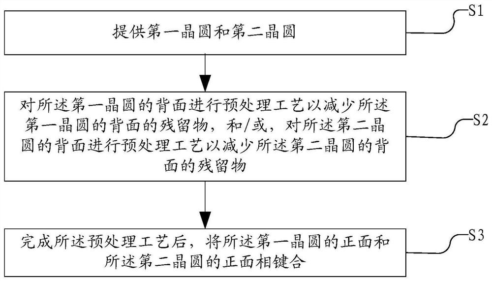
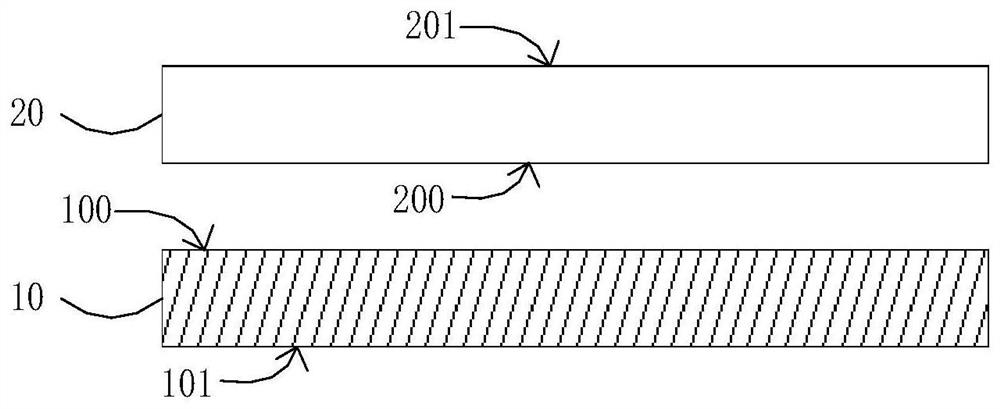
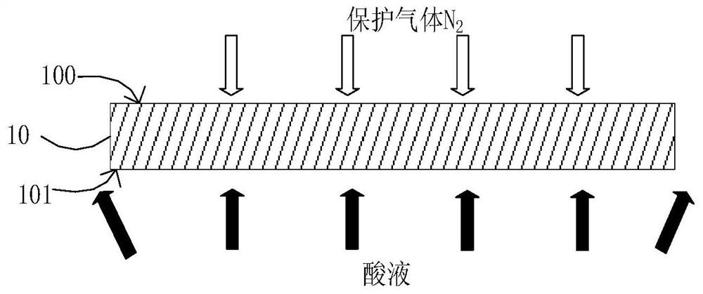
[0022] In a three-dimensional integrated circuit, such as a back-illuminated CMOS (Complementary Metal Oxide Semiconductor, Complementary Metal Oxide Semiconductor) image sensor, its manufacturing process needs to penetrate the silicon substrate to align the device wafer microlens, metal grid and substrate photodiode. The wafer bonding twist is the main factor affecting the through-wafer alignment, therefore, improving the wafer bonding twist can effectively improve the alignment accuracy of the through-wafer, thereby improving the uniformity of the bonded wafer.
[0023] The inventor obtained a wafer bonding distortion of about 70nm by measuring a lithography machine. In this wafer bonding method, after the previous process of the first wafer and the second wafer is completed, the The front side of the first wafer is bonded to the front side of the second wafer. The wafer bonding twist obtained by this wafer bonding method is relatively high, which leads to low accuracy of th...
PUM
 Abstract
Description
Claims
Application Information
 - R&D
- Intellectual Property
- Life Sciences
- Materials
- Tech Scout
- Unparalleled Data Quality
- Higher Quality Content
- 60% Fewer Hallucinations
Browse by: Latest US Patents, China's latest patents, Technical Efficacy Thesaurus, Application Domain, Technology Topic, Popular Technical Reports.
© 2025 PatSnap. All rights reserved.Legal|Privacy policy|Modern Slavery Act Transparency Statement|Sitemap|About US| Contact US: help@patsnap.com