A High Precision Resistor with Reduced Resistance Change Rate
A change rate, high-precision technology, applied in the direction of resistors, resistor assemblies, resistor components, etc., can solve the problems of unstable resistance value, unfavorable resistance, and reduced control accuracy, so as to reduce the degree of change and prolong the service life , to reduce the effect of temperature changes
- Summary
- Abstract
- Description
- Claims
- Application Information
AI Technical Summary
Problems solved by technology
Method used
Image


Examples
Embodiment 1
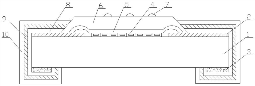
[0028] Such as figure 1 As shown, a high-precision resistor that reduces the rate of change of resistance value includes a ceramic substrate 1, a surface electrode 2, a back electrode 3, a resistor body 4, a primary protective layer 5, a secondary protective layer 6, marks 7, and terminal electrodes 8 , an intermediate electrode 9, and an external electrode 10, the resistor body 4 is arranged in the middle of the upper surface of the ceramic substrate 1, the primary protective layer 5 and the secondary protective layer 6 are sequentially stacked on the upper side of the resistor body 4 from bottom to top, and the primary The protective layer 5 covers the resistor body 4, and the secondary protective layer 6 covers the primary protective layer 5; the surface electrode 2 is arranged on the upper surface of the ceramic substrate 1, and is on both sides of the resistor body 4; on the ceramic substrate The two ends of the lower surface of 1 are provided with back electrodes 3; the ...
Embodiment 2
[0033]A high-precision resistor that reduces the rate of change of resistance value, including a ceramic substrate 1, a surface electrode 2, a back electrode 3, a resistor body 4, a primary protective layer 5, a secondary protective layer 6, a mark 7, a terminal electrode 8, and an intermediate electrode 9. External electrode 10, the resistor body 4 is arranged in the middle of the upper surface of the ceramic substrate 1, the primary protective layer 5 and the secondary protective layer 6 are stacked on the upper side of the resistor body 4 from bottom to top, and the primary protective layer 5 The resistor body 4 is covered, and the secondary protective layer 6 covers the primary protective layer 5; the surface electrode 2 is arranged on the upper surface of the ceramic substrate 1, and is on both sides of the resistor body 4; under the ceramic substrate 1 The two ends of the surface are provided with back electrodes 3; the terminal electrodes 8 cover the two ends of the cera...
Embodiment 3
[0039] Such as Figure 1 to Figure 3 , a high-precision resistor that reduces the rate of resistance change, including a ceramic substrate 1, a surface electrode 2, a back electrode 3, a resistor body 4, a primary protective layer 5, a secondary protective layer 6, marks 7, terminal electrodes 8, middle Electrodes 9 and external electrodes 10, the resistor body 4 is arranged in the middle of the upper surface of the ceramic substrate 1, the primary protective layer 5 and the secondary protective layer 6 are sequentially stacked on the upper side of the resistor body 4 from bottom to top, and the primary protective layer 5 covers the resistor body 4, and the secondary protective layer 6 covers the primary protective layer 5; the surface electrode 2 is arranged on the upper surface of the ceramic substrate 1, and is on both sides of the resistor body 4; The two ends of the lower surface are provided with back electrodes 3; the terminal electrodes 8 cover the two ends of the cera...
PUM
| Property | Measurement | Unit |
|---|---|---|
| melting point | aaaaa | aaaaa |
Abstract
Description
Claims
Application Information
 - R&D
- Intellectual Property
- Life Sciences
- Materials
- Tech Scout
- Unparalleled Data Quality
- Higher Quality Content
- 60% Fewer Hallucinations
Browse by: Latest US Patents, China's latest patents, Technical Efficacy Thesaurus, Application Domain, Technology Topic, Popular Technical Reports.
© 2025 PatSnap. All rights reserved.Legal|Privacy policy|Modern Slavery Act Transparency Statement|Sitemap|About US| Contact US: help@patsnap.com