Wafer test device, system and method

A technology for wafer testing and wafer acceptance testing, which is applied to measurement devices, single semiconductor device testing, and electrical measurement, etc. It can solve the problems of high test risk, low wafer acceptance testing efficiency, etc., and achieve high card replacement efficiency. , The effect of improving the level of automated manufacturing and improving the efficiency of testing

Inactive Publication Date: 2018-09-14
HUAIAN IMAGING DEVICE MFGR CORP
View PDF6 Cites 5 Cited by
  • Summary
  • Abstract
  • Description
  • Claims
  • Application Information

AI Technical Summary

Problems solved by technology

[0007] In view of the shortcomings of the prior art described above, the purpose of the present invention is to provide a wafer testing device, system and method for solving the problems of low wafer acceptance testing efficiency and high testing risk in the prior art

Method used


Image

  • Wafer test device, system and method
  • Wafer test device, system and method
  • Wafer test device, system and method

Examples


Embodiment 1

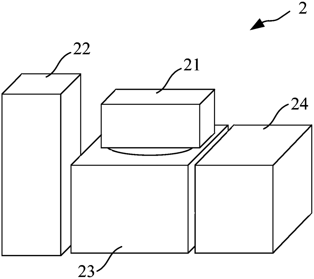
[0058] Such as image 3 As shown, the present invention provides a kind of wafer testing system 2, and described wafer testing system 2 comprises:

[0059] A wafer testing device 21 , a testing control unit 22 , a testing platform 23 and a wafer loading and unloading platform 24 .

[0060] Such as image 3 As shown, the wafer test device 21 is arranged above the test table 23, and the test structures in different directions are respectively tested by the rotation of the probe card, and different probe cards are tested by the rotation of the probe card holder. .

[0061] Specifically, as image 3 As shown, the wafer testing device 21 includes a test head 211 , a probe holder 212 , a first probe card 213 and a second probe card 214 .

[0062] More specifically, as Figure 4 and Figure 5As shown, the test head 211 carries the probe holder 212 , the first probe card 213 and the second probe card 214 . In this embodiment, the test head 211 has a cuboid structure, but in pra...

Embodiment 2

[0073] Such as Figure 3-6 As shown, the present embodiment provides a wafer testing method, which is implemented based on the wafer testing system 2, and the wafer testing method includes:

[0074] Step S1: providing a first wafer to be tested.

[0075] Specifically, the first wafer to be tested includes test structures located in the first direction and the second direction. In this embodiment, the first wafer to be tested is a wafer after the first metal layer Metal1 is completed. , the first direction and the second direction are perpendicular to each other, and are respectively longitudinal and transverse directions.

[0076] Step S2: loading the first wafer to be tested onto the test bench 23, and performing the first test in the first direction and the second direction on the first wafer to be tested respectively, the first After the test is completed, the first wafer to be tested is unloaded from the test platform 23 .

[0077] Specifically, in this embodiment, the ...


PUM


Abstract

The invention provides a wafer test device, system and method. The wafer test device comprises a test head, a probe card seat as well as first and a second probe cards, wherein the probe card seat isarranged on the lower end surface of the test head through a card seat rotating shaft; each of the first and second probe cards is arranged on the lower end surface of the probe card seat through a probe card rotating shaft, the distance between the first probe card and the card seat rotating shaft is equal to that between the second probe card and the card seat rotating shaft, and a first probe group and a second probe group are arranged on the first probe card and the second probe card respectively and used for testing to-be-tested wafers at different process stages in different directions.The to-be-tested wafers at different process stages can be tested in different directions, when test structures at the same process stage in different directions, the unloading of wafers and reloadingafter direction change are not required, and probe realignment is not required, so that the test efficiency is greatly improved. Meanwhile, when test structures at different process stages are tested, the probe cards are directly and automatically switched, the card switching efficiency is high, and the risk of human card switching mistakes is avoided.

Description

technical field [0001] The invention relates to the field of semiconductor testing, in particular to a wafer testing device, system and method. Background technique [0002] In microelectronics technology, semiconductor silicon wafers need to perform electrical tests on various test structures on the silicon wafers after the manufacturing process is completed. This test is called Wafer Acceptance Test (WAT). By analyzing the test data obtained from the wafer acceptance test, problems in the semiconductor process technology can be found to help the process process to be adjusted. [0003] The probe card and test head in the traditional wafer acceptance testing machine are fixed, such as figure 1 and figure 2 As shown, the probe card 12 is arranged on the lower surface of the test head 11, and the two are fixedly connected without any relative movement; the probe card 12 is provided with a probe 13, and the two are also fixed. connected without any relative movement. In t...

Claims


Application Information

Patent Timeline
Patent Type & Authority Applications(China)
IPC IPC(8): G01R31/26G01R1/067
CPCG01R1/067G01R31/26
Inventor 叶定文汪海
Owner HUAIAN IMAGING DEVICE MFGR CORP
Why Eureka
Try Eureka