Display substrate, repair method thereof, and display device
A technology for a display substrate and a repair method, which is applied in the directions of organic semiconductor devices, semiconductor devices, electrical components, etc., and can solve problems such as affecting multiple sub-pixels.
- Summary
- Abstract
- Description
- Claims
- Application Information
AI Technical Summary
Problems solved by technology
Method used
Image
Examples
Embodiment 1
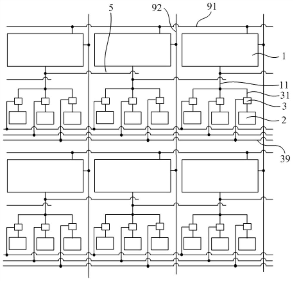
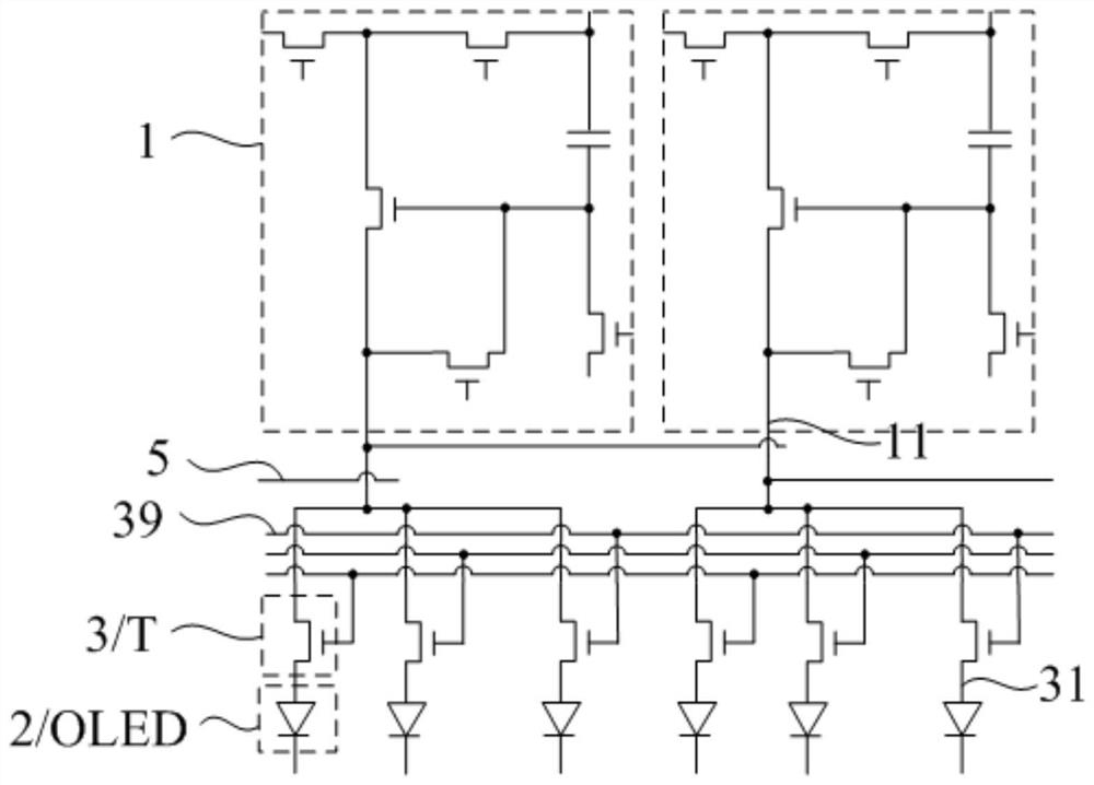
[0034] Such as Figure 1 to Figure 3 As shown, this embodiment provides a display substrate, which includes a plurality of driving units 1 for driving the display unit 2 to display, each driving unit 1 corresponds to a plurality of display units 2, and the output terminal 11 of each driving unit 1 The corresponding display units 2 are respectively connected via a branch circuit 31 having a switch unit 3 .
[0035] In the display substrate of this embodiment, the display unit 2 is the part that actually performs light-emitting display, which is equivalent to the light-emitting part in the sub-pixel, and the driving unit 1 is used to provide the display unit 2 with driving signals (such as current, voltage, etc.) To control its light emission, it is equivalent to the pixel circuit of each sub-pixel. Moreover, the output terminal 11 of each drive unit 1 is connected to a plurality of display units 2 through a plurality of branches 31, and each branch 31 is provided with a switch...
Embodiment 2
[0065] Such as Figure 1 to Figure 3 As shown, this embodiment provides a method for repairing the above-mentioned display substrate, which includes:
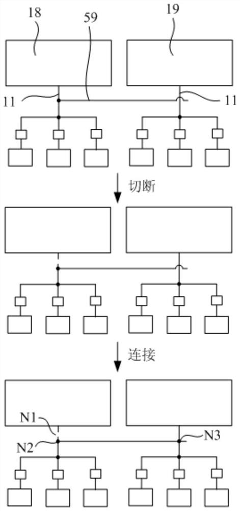
[0066] S01. Find the drive unit 1 that cannot drive the display unit 2 to display, take it as the problem drive unit 18, select a repair line 5 corresponding to the problem drive unit 18 as the target repair line 59, and use another driver corresponding to the target repair line 59 Unit 1 is the target drive unit 19 .
[0067] S02, cut off the connection between the output terminal 11 of the problem driving unit 18 and its corresponding display units 2, and connect the target repair line 59 with the output terminal 11 of the problem driving unit 18 and the target driving unit 19, so that the target driving unit 19 is connected to the problem Each display unit 2 corresponding to the drive unit 18 is connected.
[0068] That is to say, the drive unit 1 (problem drive unit 18 ) that cannot be driven due to a fault is determined ...
Embodiment 3
[0076] This embodiment provides a display device, which includes the above-mentioned display substrate.
[0077] That is to say, the above display substrates (including unrepaired and repaired ones) can be combined with other components to form a completed display device.
[0078] Specifically, the display device can be any product with a display function such as a liquid crystal display panel, an organic light-emitting diode (OLED) display panel, an electronic paper, a mobile phone, a tablet computer, a television set, a monitor, a notebook computer, a digital photo frame, a navigator, or the like. part.
[0079] Of course, it should be understood that after repairing, the driving method of the above display device (that is, the way of supplying signals to each line) has no substantial change, but under the same driving method, the signal transmission of the position where repairing occurs The way naturally changes.
PUM
 Abstract
Description
Claims
Application Information
 - R&D
- Intellectual Property
- Life Sciences
- Materials
- Tech Scout
- Unparalleled Data Quality
- Higher Quality Content
- 60% Fewer Hallucinations
Browse by: Latest US Patents, China's latest patents, Technical Efficacy Thesaurus, Application Domain, Technology Topic, Popular Technical Reports.
© 2025 PatSnap. All rights reserved.Legal|Privacy policy|Modern Slavery Act Transparency Statement|Sitemap|About US| Contact US: help@patsnap.com


