Semiconductor packaging detection equipment

A technology for testing equipment and semiconductors, applied in packaging, packaging protection, transportation and packaging, etc., can solve the problems of low quality efficiency and errors of semiconductor marking, and achieve the effect of saving manpower, high efficiency and convenient operation.

Pending Publication Date: 2018-10-02
重庆市嘉凌新科技有限公司
View PDF0 Cites 1 Cited by
  • Summary
  • Abstract
  • Description
  • Claims
  • Application Information

AI Technical Summary

Problems solved by technology

[0004] The present invention intends to provide semiconductor packaging testing equipment to solve the

Method used


Image

  • Semiconductor packaging detection equipment

Examples


Embodiment 1

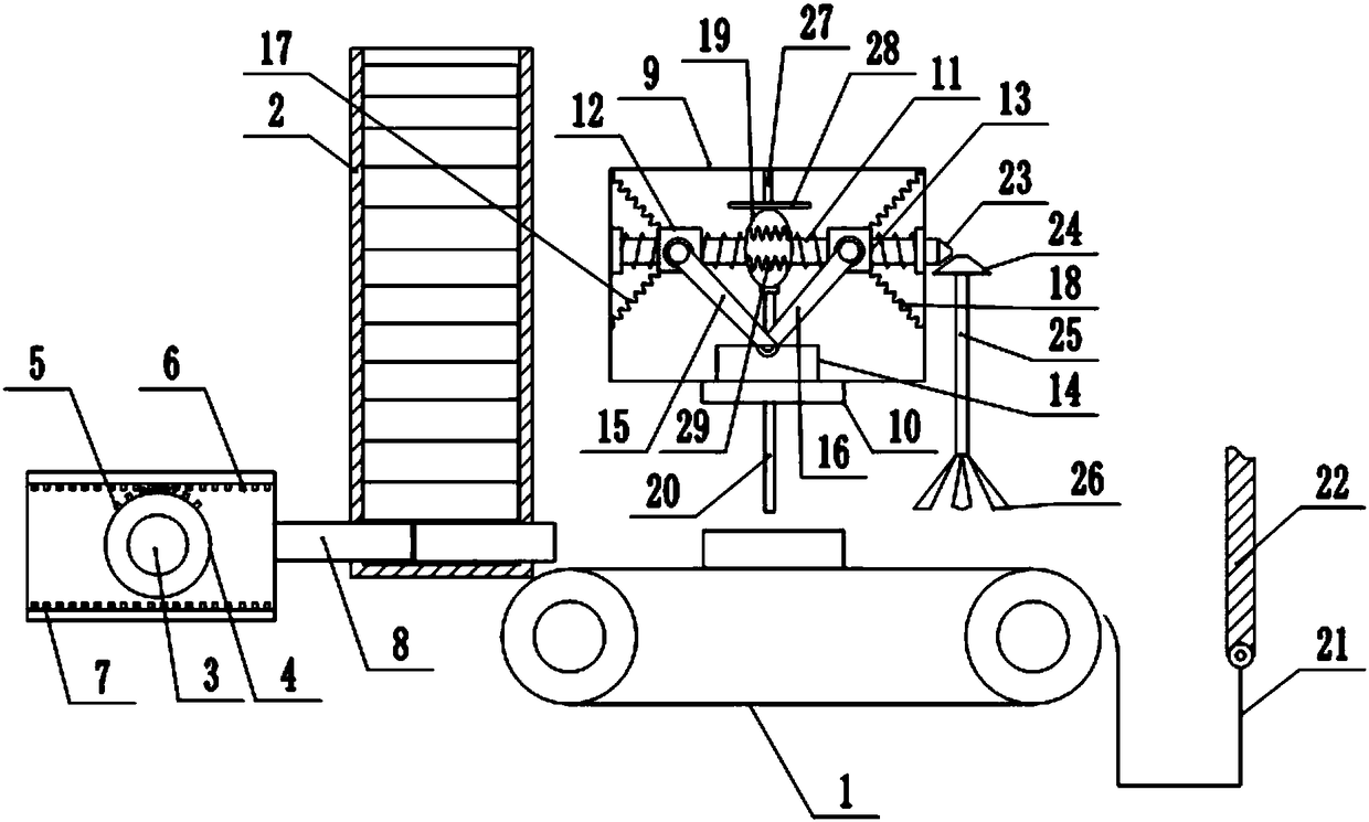
[0020] The embodiment is basically as attached figure 1 Shown: Semiconductor packaging and testing equipment, including a frame and a conveyor belt 1, the conveyor belt 1 is connected with a stepping motor, the left side of the conveyor belt 1 is provided with a drive mechanism, the drive mechanism includes a storage box 2, and the bottom of the right wall of the storage box 2 is provided with The discharge port, the discharge port and the feed end of the conveyor belt 1 are arranged oppositely, and the bottom of the left wall of the storage box 2 is correspondingly provided with a drive port, and the frame is connected with a drive shaft 3 for rotation, and the drive shaft 3 is connected with a drive motor. The shaft 3 is coaxially fixedly connected with the driving disc 4, and the driving disc 4 is provided with a section of gear teeth 5, and the frame is slidably connected with a rectangular gear frame, and the rectangular gear frame is provided with an upper rack 6 and a lo...

Embodiment 2

[0029] The difference between Embodiment 2 and Embodiment 1 is that the marking on the package is manually identified. When the marking paste is manually recognized, the drive motor is manually turned on, so that the device can mark and seal the package with blurred marking. separate.


PUM


Abstract

The invention relates to semiconductor packaging detection equipment. The equipment comprises a machine frame and a conveying belt, a driving mechanism is arranged on one side of the conveying belt, the driving mechanism comprises a storage box, a discharging opening is formed in the bottom of the storage box, and the discharging opening is arranged right opposite to the feeding end of the conveying belt; a shell body is arranged above the conveying belt, a color mark sensor is fixedly connected to the outer side of the bottom of the shell body, and a light outlet of the color mark sensor is right opposite to the belt face of the conveying belt; a bidirectional screw rod is rotationally connected inside the shell body, and is connected with a first motor, and the first motor is controlledby the color mark sensor; the two ends of the bidirectional screw rod are in threaded connection with a left-handed nut and a right-handed nut respectively, an elastic liquid storage bag is arranged in the middle of the bidirectional screw rod in a sleeving mode, a liquid outlet pipe is arranged on the elastic liquid storage bag in a communicating mode, and the bottom end of the liquid outlet pipepenetrates through the shell body and is right opposite to the belt surface of the conveying belt; and a collecting box is arranged at the discharging end of the conveying belt, and a magnetic plateis rotationally connected to the side wall of the collecting box. The semiconductor packaging detection equipment is accurate in detection and high in efficiency.

Description

technical field [0001] The invention relates to the field of semiconductor processing, in particular to semiconductor package testing equipment. Background technique [0002] A semiconductor refers to a material whose conductivity at room temperature is between that of a conductor and an insulator. Semiconductors have a wide range of applications in radios, televisions, and temperature measurement. During the processing of semiconductors, processes such as welding, packaging, and cutting are usually performed. Semiconductor packaging refers to the process of processing the tested wafers according to the product model and functional requirements to obtain independent chips. [0003] After semiconductor packaging, in order to distinguish the model of the package and the manufacturer, it is usually necessary to print a mark on the package, and after printing the mark, it is necessary to inspect and monitor the quality of the mark, and remove the fuzzy mark to ensure that the ...

Claims


Application Information

Patent Timeline
IPC IPC(8): B65B57/04
CPCB65B57/04
Inventor 罗妍
Owner 重庆市嘉凌新科技有限公司
Why Eureka
Try Eureka