Nanometer microcrystal mixed optical structure back projection high-definition image film and back projection screen

A nano-crystal, optical structure technology, applied in the field of optical projection, can solve the problems of unclear viewing, unclear imaging images, glare, etc.

Pending Publication Date: 2018-10-02
中科宝溢视觉科技(江苏)有限公司
View PDF5 Cites 4 Cited by
  • Summary
  • Abstract
  • Description
  • Claims
  • Application Information

AI Technical Summary

Problems solved by technology

[0003] However, in reality, the projection screen often works in a bright environment, and its surface is very easy to be affected by strong light, resulting in unclear, uneven, glare, and severe white fog in the imaging pictur...

Method used


Image

  • Nanometer microcrystal mixed optical structure back projection high-definition image film and back projection screen

Examples


Embodiment 1

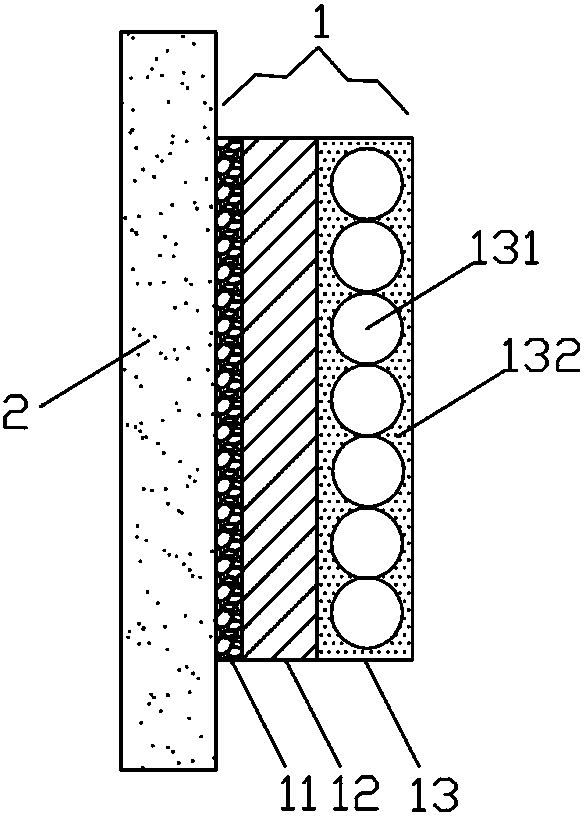
[0021] Such as figure 1 As shown, the first technical solution of this embodiment is specifically: a rear-projection high-definition image film 1 with a nano-microcrystal mixed optical structure, including a base layer 12, a nano-crystal and nano-bead hybrid imaging coating 13 and a rear projection film 1. Adhesive layer 11, the nano-crystal and nano-bead mixed imaging coating 13 is formed by mixing nano-crystal 132 and nano-bead 131 in proportion and uniformly coating on one side of the base layer 12, so The above-mentioned adhesive layer 11 is arranged on the other side of the base layer 12 for pasting on an external support. It should be noted that the external support here refers to glass, acrylic and other transparent and stickable carriers with suitable areas. (In Example 2, AG glass is selected as the external support, refer to Example 2 for details).

[0022] It should be pointed out that the nanometer microbeads 131 are optical microbeads, which act on the diffractio...

Embodiment 2

[0029] This embodiment is based on the rear projection screen of Embodiment 2, such as figure 1 As shown, it specifically includes the nano-microcrystalline mixed optical structure rear projection high-definition image film 1 and AG glass 2, and the back adhesive layer 11 of the nano-crystalline mixed optical structure rear projection high-definition image film 1 is pasted on the AG glass 2 On the bright side, it should be pointed out that the AG glass 2 is treated on the reflective surface of the original glass to a matte non-reflective surface. Compared with ordinary glass, AG glass has a lower reflectance, and the reflectance of light is increased by 8%. Reduced to less than 1%, so AG glass can form a clear and transparent visual effect, and achieve the ideal purpose of resisting reflection of ambient light and anti-glare protection.

[0030] In this embodiment, the thickness of the AG glass 2 is between 2-10 mm, and the optimum thickness in this embodiment is 4 mm.

[003...


PUM

PropertyMeasurementUnit
Particle sizeaaaaaaaaaa
Thicknessaaaaaaaaaa

Abstract

The invention discloses a nanometer microcrystal mixed optical structure back projection high-definition image film. The nanometer microcrystal mixed optical structure back projection high-definitionimage film comprises a substrate layer, a nanometer microcrystal and nanometer micro ball mixed imaging coating layer and a back adhesive layer; the nanometer microcrystal and nanometer micro ball mixed imaging coating layer is formed by uniformly coating one surface of the substrate layer with nanometer microcrystal, nanometer micro balls and an adhesive based on a proportion; and the back adhesive layer is arranged on the other surface of the substrate layer for pasting external supports. The nanometer microcrystal and the nanometer micro balls are mixed and coated on the substrate layer, sothat compared with an image film with separated inorganic silicon particle coating layer and glass micro ball coating layer, the image film disclosed in the invention can eliminate projector light source light spots in a more all-around manner, the image angle of visibility can be enlarged to 178 degrees, and brightness, color saturation degree and light resistance and eye protection performanceof the projection image are improved, so that the image film is applicable to all projectors of different lenses on the market.

Description

technical field [0001] The invention relates to the field of optical projection technology, in particular to a rear-projection high-definition image film and a rear-projection screen with a nano-microcrystalline mixed optical structure. Background technique [0002] Nowadays, projection technology is widely used in life and work, especially in large conference rooms, command and control centers, training and education structures, exhibition halls, exhibition halls, airports, window displays and other important occasions. [0003] However, in reality, projection screens often work in bright environments, and their surfaces are easily affected by strong light, resulting in unclear, uneven, glare, and severe white fog-like images. And these phenomena will greatly reduce the contrast and brightness of the picture, which will easily cause the user to see it unclearly, seriously affect the perception, and easily lose its own display, demonstration or advertising effect. [0004] ...

Claims


Application Information

Patent Timeline
IPC IPC(8): G03B21/60G03B21/62
CPCG03B21/60G03B21/62
Inventor 张保平衡梁臧慧玲
Owner 中科宝溢视觉科技(江苏)有限公司
Why Eureka
Try Eureka