Pixel unit and manufacturing method thereof, array substrate and display device

A technology for a pixel unit and a manufacturing method, which can be used in semiconductor/solid-state device manufacturing, electrical components, instruments, etc., and can solve problems such as less overlap

Active Publication Date: 2021-04-27
BOE TECH GRP CO LTD +1
View PDF4 Cites 0 Cited by
  • Summary
  • Abstract
  • Description
  • Claims
  • Application Information

AI Technical Summary

Problems solved by technology

[0006] However, if figure 1 As shown, there is very little overlap between the pixel electrode 200 and the common electrode 300, and it is difficult to electrically connect the two without affecting the normal display.

Method used


Image

  • Pixel unit and manufacturing method thereof, array substrate and display device
  • Pixel unit and manufacturing method thereof, array substrate and display device
  • Pixel unit and manufacturing method thereof, array substrate and display device

Examples


Embodiment Construction

[0043] Specific embodiments of the present invention will be described in detail below in conjunction with the accompanying drawings. It should be understood that the specific embodiments described here are only used to illustrate and explain the present invention, and are not intended to limit the present invention.

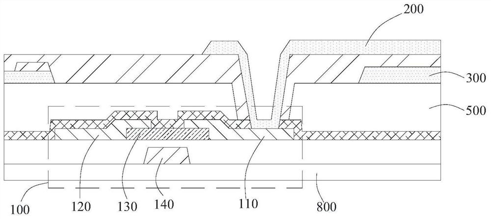
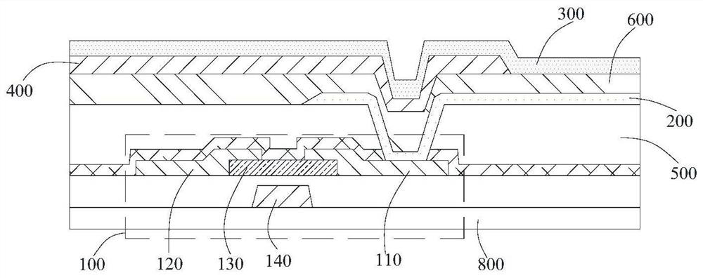
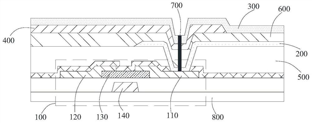
[0044] As an aspect of the present invention, a pixel unit is provided, such as figure 2 As shown, the pixel unit includes a thin film transistor 100, a pixel electrode 200, a first insulating layer 500, a second insulating layer 600, a common electrode and a common electrode line 400, and the common electrode line 400 is electrically connected to the common electrode. The first insulating layer 500 is disposed between the layer where the drain 110 of the thin film transistor 100 is located and the pixel electrode layer, the pixel electrode 200 is electrically connected to the drain 110 through a via hole penetrating through the first insulating layer 500, and ...


PUM


Abstract

The present invention provides a pixel unit, wherein the pixel unit includes a thin film transistor, a pixel electrode, a first insulating layer, a second insulating layer, a common electrode and a common electrode line, and the common electrode line is electrically connected to the common electrode , the first insulating layer is disposed between the drain of the thin film transistor and the pixel electrode, the pixel electrode is electrically connected to the drain through a via hole penetrating through the first insulating layer, and the first Two insulating layers are disposed between the pixel electrode and the common electrode line to insulate the pixel electrode from the common electrode line, and a part of the second insulating layer and a part of the common electrode line are located in the vias. The invention also provides an array substrate, a display device, and a manufacturing method of a pixel unit. When an abnormal bright spot occurs in the pixel unit, it is convenient to perform a dark spot restoration operation on the pixel unit.

Description

technical field [0001] The present invention relates to the field of display technology, in particular, to a pixel unit, a method for manufacturing the pixel unit, an array substrate including the pixel unit, and a display device including the array substrate. Background technique [0002] The display panel includes a plurality of pixel units, figure 1 Shown in is a schematic cross-sectional view of a pixel unit of a display panel. As shown in the figure, the pixel unit includes a thin film transistor 100 formed on a base substrate 800 , a first insulating layer 500 , a common electrode 300 and a pixel electrode 200 . The thin film transistor 100 includes a drain 110 , a source 120 , a gate 140 and an active layer 130 . It is easy to understand that there is an insulating space between the gate 140 and the active layer 130 . The provision of the first insulating layer 500 can reduce parasitic capacitance and line delay, and generally the first insulating layer 500 is made...

Claims


Application Information

Patent Timeline
Patent Type & Authority Patents(China)
IPC IPC(8): G02F1/1362G02F1/1333G02F1/1343
CPCG02F1/133345G02F1/134363G02F1/136227G02F1/136259G02F1/136286H01L27/124H01L22/12H01L29/41733H01L27/1248H01L27/1288H01L27/1222H01L21/76894H01L29/78669H01L29/66765H01L22/14
Inventor 任兴凤车璐曾玲玲
Owner BOE TECH GRP CO LTD
Why Eureka
Try Eureka