An array substrate, a touch display panel and a touch display device

An array substrate and display area technology, applied in static indicators, instruments, calculations, etc., can solve the problems of poor brightness uniformity of special-shaped display panels and uneven brightness of notch display areas, so as to reduce intensity, improve brightness uniformity, The effect of reducing brightness differences

Active Publication Date: 2021-07-16
XIAMEN TIANMA MICRO ELECTRONICS
View PDF6 Cites 0 Cited by
  • Summary
  • Abstract
  • Description
  • Claims
  • Application Information

AI Technical Summary

Problems solved by technology

[0004] In view of this, the present invention provides an array substrate, a touch display panel and a touch display device to solve the problems of the irregular display panel caused by the inconsistency between the brightness of the notched display area and the brightness of the conventional display area in the existing irregular display panel. The problem of poor brightness uniformity

Method used


Image

  • An array substrate, a touch display panel and a touch display device
  • An array substrate, a touch display panel and a touch display device
  • An array substrate, a touch display panel and a touch display device

Examples


Embodiment Construction

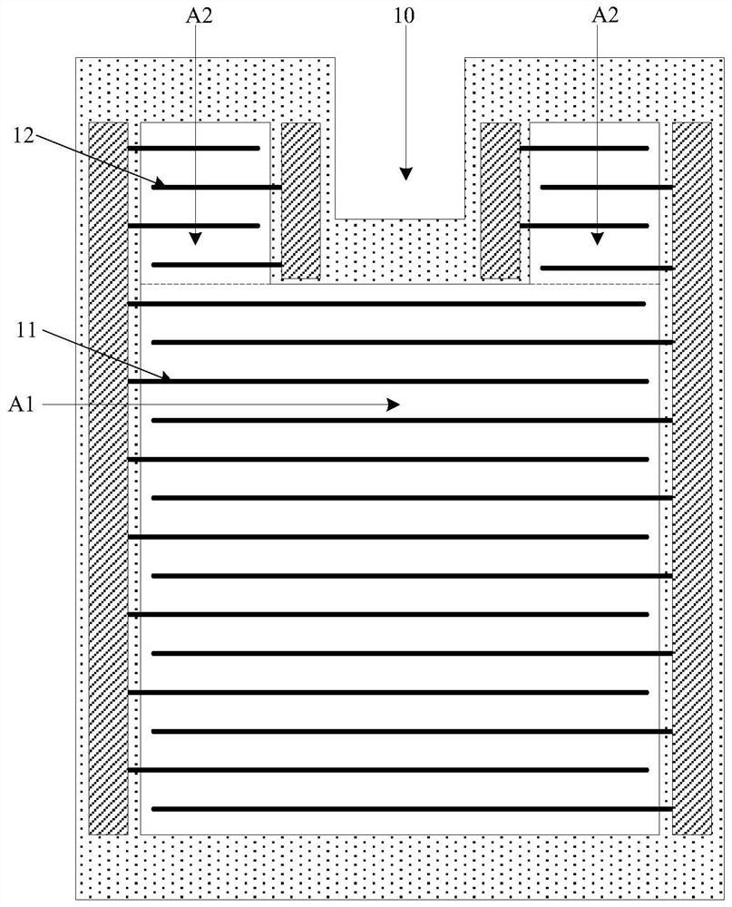
[0029] As described in the background technology, the brightness of the notch display area A2 of the special-shaped display panel is inconsistent with the brightness of the regular display area A1, that is, the brightness of the notch display area A2 is greater than the brightness of the regular display area A1. The reason is that the length of the second scan line 12 in the notch display area A2 is shorter than the length of the first scan line 11 in the normal display area A1, so that the attenuation of the scan signal on the second scan line 12 is smaller, that is, the second scan line 12 outputs The intensity of the scanning signal to the pixels in the notch display area A2 connected to it is greater than the intensity of the scanning signal output by the first scan line 11 to the pixels in the conventional display area A1 connected to it, so that the data writing of the pixels in the notch display area A2 The input time is longer than the data writing time of the pixels in...


PUM


Abstract

The present invention provides an array substrate, a touch display panel and a touch display device. The number of inverters in the second cache unit is smaller than the number of inverters in the first cache unit, or, the number of inverters in the second cache unit The size of the inverter is smaller than the size of the inverter in the first cache unit, or the number of inverters in the second cache unit is smaller than the number of inverters in the first cache unit, and the inverter in the second cache unit The size of the phaser is smaller than the size of the inverter in the first buffer unit, therefore, by reducing the signal amplification effect of the second buffer unit in the second shift register unit, the transmission of the second shift register unit to the second The intensity of the scanning signal of the scanning line, so that the intensity difference between the intensity of the scanning signal output by the first scanning line and the intensity of the scanning signal output by the second scanning line can be reduced, and then the brightness of the conventional display area and the brightness of the notch display area can be reduced difference, improving the brightness uniformity of the display panel.

Description

technical field [0001] The present invention relates to the technical field of display devices, and more specifically, to an array substrate, a touch display panel and a touch display device. Background technique [0002] With the development of display technology, people not only have higher and higher requirements for the function of the display panel, but also higher and higher requirements for the appearance. In order to better adapt to the overall changes in the environment and usage requirements, special-shaped display panels have emerged. [0003] Such as figure 1 as shown, figure 1 It is a top-view structure schematic diagram of an existing special-shaped display panel. The edge of the special-shaped display panel extending in the same direction as the scanning line has a notch 10, and the notch 10 divides the display area of ​​the special-shaped display panel into a regular display area A1 and a display area located in the notch. The gaps on both sides of 10 disp...

Claims


Application Information

Patent Timeline
Patent Type & Authority Patents(China)
IPC IPC(8): G09G3/20G09G3/3266G09G3/36
CPCG09G3/20G09G3/3266G09G3/3674G09G2320/0233G09G2310/0286G09G2310/0291G09G2300/0426G06F3/0412
Inventor 王雨谢振清孙莹刘冰萍许育民陈国照黄敏
Owner XIAMEN TIANMA MICRO ELECTRONICS
Why Eureka
Try Eureka