Novel ceramic plug and electrostatic chuck device having the novel ceramic plug

A ceramic plug, a new type of technology, is used in the manufacture of circuits, electrical components, semiconductors/solid-state devices, etc. It can solve problems such as electrostatic chucks and wafer damage, and achieve the effect of preventing arcing and avoiding damage

Active Publication Date: 2018-10-12
BEIJING U PRECISION TECH
View PDF6 Cites 3 Cited by
  • Summary
  • Abstract
  • Description
  • Claims
  • Application Information

AI Technical Summary

Problems solved by technology

When the ceramic plug with this structure is applied to the base body, it is very likely that the gas medium in the through-cooling air hole will be broken down to cause an arc, which will damage the electrostatic chuck and the wafer.

Method used


Image

  • Novel ceramic plug and electrostatic chuck device having the novel ceramic plug
  • Novel ceramic plug and electrostatic chuck device having the novel ceramic plug
  • Novel ceramic plug and electrostatic chuck device having the novel ceramic plug

Examples


Embodiment Construction

[0019] In order to make the technical problems, technical solutions and advantages to be solved by the present invention clearer, the following will describe in detail with reference to the drawings and specific embodiments.

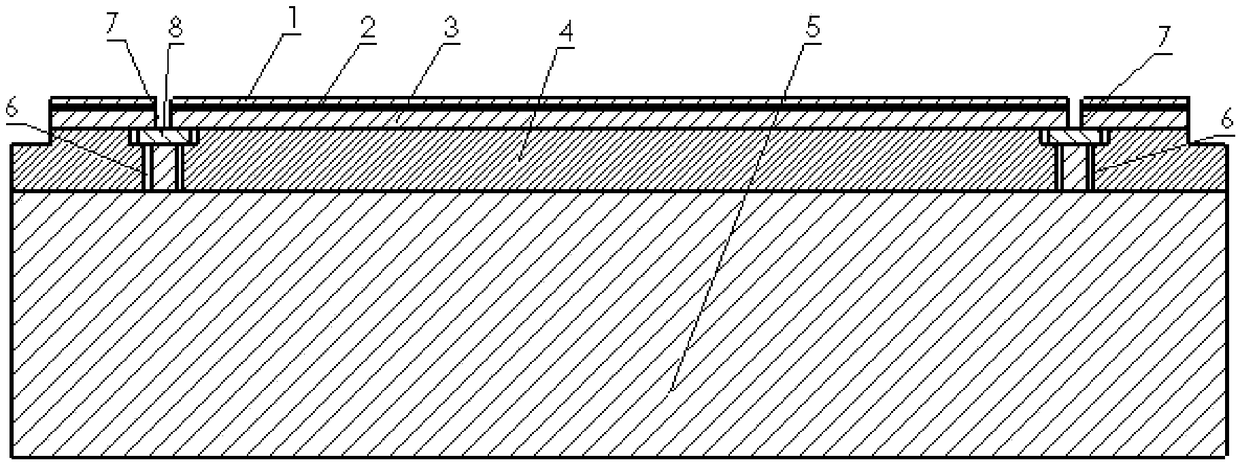
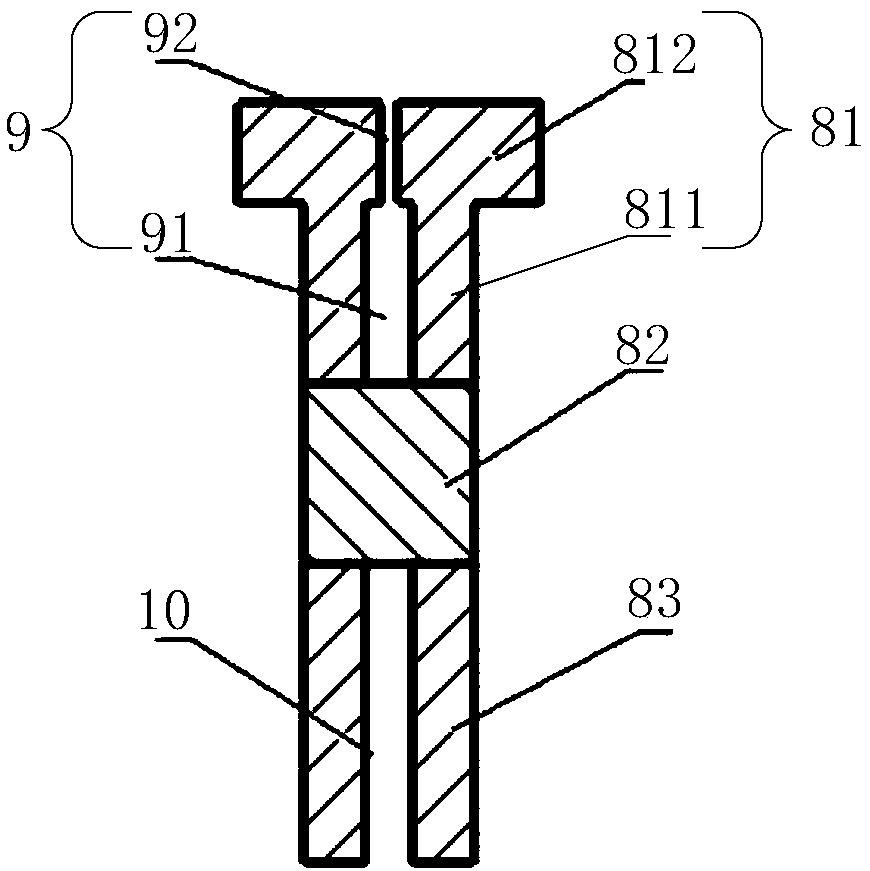
[0020] On the one hand, the present invention provides a kind of novel ceramic plug, such as image 3 As shown, it includes a ceramic plug upper part 81, a porous ceramic column 82 and a ceramic sleeve 83 connected sequentially from top to bottom. The ceramic plug upper part 81 includes a cylindrical part 812 and an annular boss part 811 arranged on the upper part of the cylindrical part 812. A first cooling gas hole 91 is disposed in the middle of the boss portion 811 , a second cooling gas hole 92 is disposed in the middle of the cylindrical portion 812 , and a third cooling gas hole 10 is disposed in the middle of the ceramic sleeve 83 .

[0021] The novel ceramic plug of the present invention includes the upper part of the ceramic plug, the porous ce...


PUM

PropertyMeasurementUnit
Diameteraaaaaaaaaa
Diameteraaaaaaaaaa
Hole depthaaaaaaaaaa

Abstract

The invention discloses a novel ceramic plug and an electrostatic chuck device having the novel ceramic plug, belonging to the field of semiconductor wafer processing equipment. The novel ceramic plugincludes an upper portion of the ceramic plug, a porous ceramic column and a ceramic sleeve connected in order from top to bottom, wherein the upper portion of the ceramic plug includes a cylindricalportion and an annular boss portion disposed at the upper portion of the cylindrical portion, the middle portion of the annular boss portion is provided with a first cooling gas hole, the middle portion of the cylindrical portion is provided with a second cooling gas hole, and the middle portion of the ceramic sleeve is provided with a third cooling gas hole. The invention is capable of avoidingthe arc phenomena generated at the cooling gas holes of the cooling gas uniformly distributing plate of the electrostatic chuck.

Description

technical field [0001] The invention relates to the field of semiconductor wafer processing devices, in particular to a novel ceramic plug and an electrostatic chuck device with the novel ceramic plug. Background technique [0002] Electrostatic chucks have many advantages over traditional mechanical and vacuum chucks. Therefore, in the semiconductor production process, electrostatic chucks are often used to fix and support the wafer to avoid movement or misalignment of the wafer during the production process. However, when the electrostatic chuck is used in some processes with radio frequency bias, such as etching and physical vapor deposition processes, arcing often occurs at the pores of the electrostatic chuck. [0003] figure 1 Shown is a schematic structural diagram of an electrostatic chuck, including a dielectric layer 1, a DC electrode layer 2, an insulating layer 3, a cooling gas uniform distribution plate 4, and a base 5, which are located on the dielectric laye...

Claims


Application Information

Patent Timeline
IPC IPC(8): H01L21/683
CPCH01L21/6833
Inventor 唐娜娜杨鹏远王建冲韩玮琦侯占杰张玉利黎远成荣吉平姜鑫李金亮
Owner BEIJING U PRECISION TECH
Why Eureka
Try Eureka