A kind of pulse power source and semiconductor device

A pulsed power source, semiconductor technology, applied in vacuum evaporation plating, coating, discharge tube, etc., can solve the problems of matcher 8 mismatch, process stop, impedance can not keep up, etc., to improve stability and improve impedance Stability, ensuring the effect of impedance matching

Active Publication Date: 2020-02-14
BEIJING NAURA MICROELECTRONICS EQUIP CO LTD
View PDF5 Cites 0 Cited by
  • Summary
  • Abstract
  • Description
  • Claims
  • Application Information

AI Technical Summary

Problems solved by technology

[0005] Since the radio frequency pulse power supply 9 generates discontinuous pulse signals, the impedance detection device in the matching device 8 determines the impedance by collecting voltage and current signals, and the voltage and current signals are continuous signals, so the impedance detected by the anti-detection device cannot keep up The change of the pulse signal will cause the mismatch of the matcher 8, and then stop the whole process, especially in the case of low duty cycle and high pulse frequency, the mismatch of the matcher 8 will be more obvious

Method used


Image

  • A kind of pulse power source and semiconductor device
  • A kind of pulse power source and semiconductor device
  • A kind of pulse power source and semiconductor device

Examples


Embodiment 1

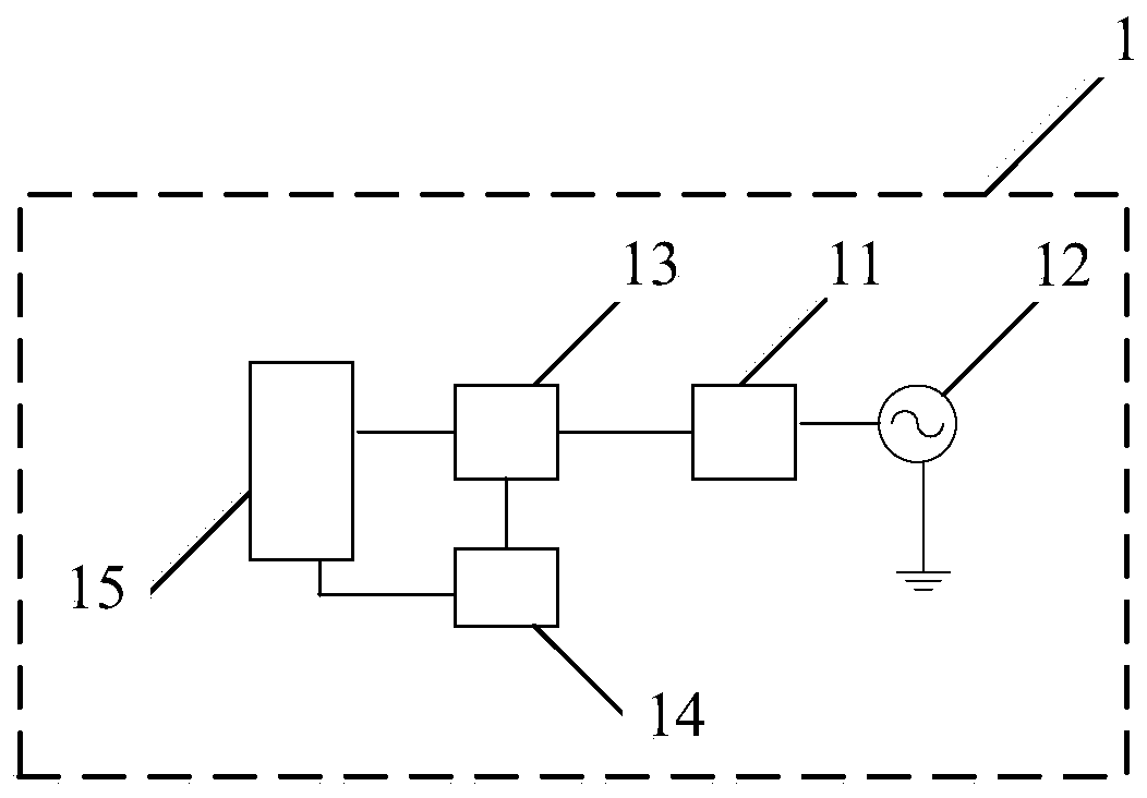
[0060] Such as Figure 2a As shown, Embodiment 1 of the present invention provides a pulsed power source 1 , including a matching unit 11 , and also includes a continuous wave power source 12 , a power divider 13 , a first phase shifter 14 and a first power combiner 15 . The power divider 13 has at least two output terminals, and the first power combiner 15 has at least two input terminals.

[0061] The input end and the output end of the matcher 11 are respectively connected with the output end of the continuous wave power source 12 and the input end of the power divider 13, and the first output end of the power divider 13 is connected with the first input end of the first power combiner 15 The second output end of the power splitter 13 is connected to the second input end of the first power combiner 15 via the first phase shifter 14 .

[0062] The continuous wave power signal output by the continuous wave power source 12 is distributed into at least two power signals by the...

Embodiment 2

[0077] Embodiment 2 of the present invention provides a pulsed power source. The difference between Embodiment 2 and Embodiment 1 is that a set of phase shifters and power combiners are added, thereby increasing a set of radio frequency pulse signal outputs.

[0078] Such as Figure 2b As shown, Embodiment 2 provides a pulsed power source 2, including a matcher 21, a continuous wave power source 22, a power divider 23, a second phase shifter 24, a second power combiner 25, and a third phase shifter 26 and a third power combiner 27 . The power divider 23 has at least four output terminals, and the second power combiner 25 and the third power combiner 27 have at least two input terminals.

[0079] The input end and the output end of the matcher 21 are connected with the output end of the continuous wave power source 22 and the input end of the power divider 23 respectively, and the first output end of the power divider 23 is connected with the first input end of the second powe...

Embodiment 3

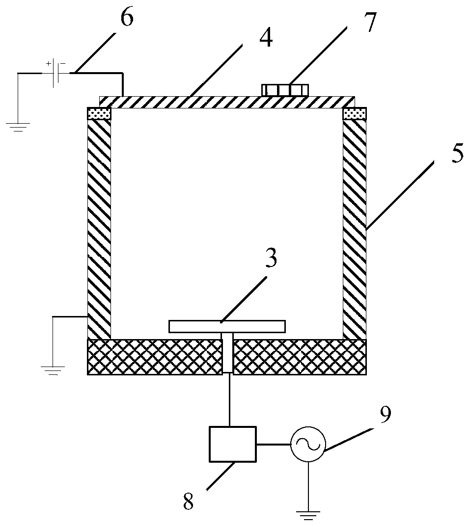
[0087] Such as image 3 As shown, embodiment 3 provides a kind of semiconductor equipment, and described semiconductor equipment is physical vapor deposition equipment, comprises pulse power source 1, reaction chamber 5, base 3 and target material 4, and target material 4 and reaction chamber 5 The side walls are sealed and connected, and the base 3 is accommodated in the reaction chamber 5 . Pulse power source 1 is the pulse power source that embodiment 1 provides, and wherein, pulse power source 1 is one, the output end of pulse power source 1 (that is the output end of first power combiner 15) and described physical vapor deposition equipment The base 3 is connected.

[0088] The semiconductor device also includes a DC power supply 6 and a magnetron 7. The DC power supply 6, the target 4 and the magnetron 7 form an upper electrode. The DC power supply 6 applies DC power to the target 4 to generate plasma.

[0089] In embodiment 3, the pulse power source 1 in embodiment 1 ...


PUM


Abstract

The present invention provides a pulsed power source and a semiconductor device, wherein an existing radio frequency (RF) pulsed power supply is replaced by a continuous wave power source, and a continuous wave power signal outputted by the continuous wave power source is allowed to pass through a matcher first, which allows a continuous voltage and current signal to be detected by an impedance detection device in the matcher, thereby avoiding the problem of impedance mismatch. Then, the matched continuous wave power signal is decomposed into at least two signals by a power divider. One of thesignals is phase-shifted by a phase shifter and then superimposed with the remaining signals to obtain a RF pulse signal. In this way, the RF pulse signal can be generated and pulsed RF energy can beused in the process to reduce plasma-induced damage. The impedance matching can also be guaranteed, thus the stability of the matching device can be improved, so as to further improve the impedance stability of a reaction chamber. Especially in the case of low duty cycle and high pulse frequencies, the effect of improving the stability of the matcher is more significant.

Description

technical field [0001] The invention relates to the technical field of semiconductor equipment manufacturing, in particular to a pulse power source and semiconductor equipment. Background technique [0002] In semiconductor coating and etching equipment, the RF energy provided by the RF power supply is usually transmitted into the chamber to ionize the gas in a high vacuum state (such as argon, helium, nitrogen, hydrogen, etc.) to generate a large amount of electrons Plasma of active particles such as ions, atoms, molecules and free radicals in the excited state, complex interactions between these active particles and the wafer placed in the cavity and exposed to the plasma environment, make the surface of the wafer material Various physical and chemical reactions occur, thereby changing the surface properties of the material, and completing the coating and etching process of the wafer. [0003] Because the pulsed plasma technology can reduce the plasma-induced damage (Plas...

Claims


Application Information

Patent Timeline
Patent Type & Authority Patents(China)
IPC IPC(8): H01J37/32C23C14/22C23C14/35C23C14/56
CPCC23C14/22C23C14/35C23C14/56H01J37/32H01J37/32431
Inventor 师帅涛
Owner BEIJING NAURA MICROELECTRONICS EQUIP CO LTD
Why Eureka
Try Eureka