Optical element, display deVice, and electronic deVice
A technology of optical components and electronic equipment, applied in optics, nonlinear optics, instruments, etc., can solve problems affecting the performance of optical components, uneven distribution of charged particles, poor control of size and connection time, etc., to achieve stable response, good optical effect
- Summary
- Abstract
- Description
- Claims
- Application Information
AI Technical Summary
Problems solved by technology
Method used
Image
Examples
Embodiment Construction
[0030] The technical solution of the present invention will be further described in detail below in conjunction with the accompanying drawings and specific embodiments, so that those skilled in the art can better understand the present invention and implement it, but the examples given are not intended to limit the present invention.
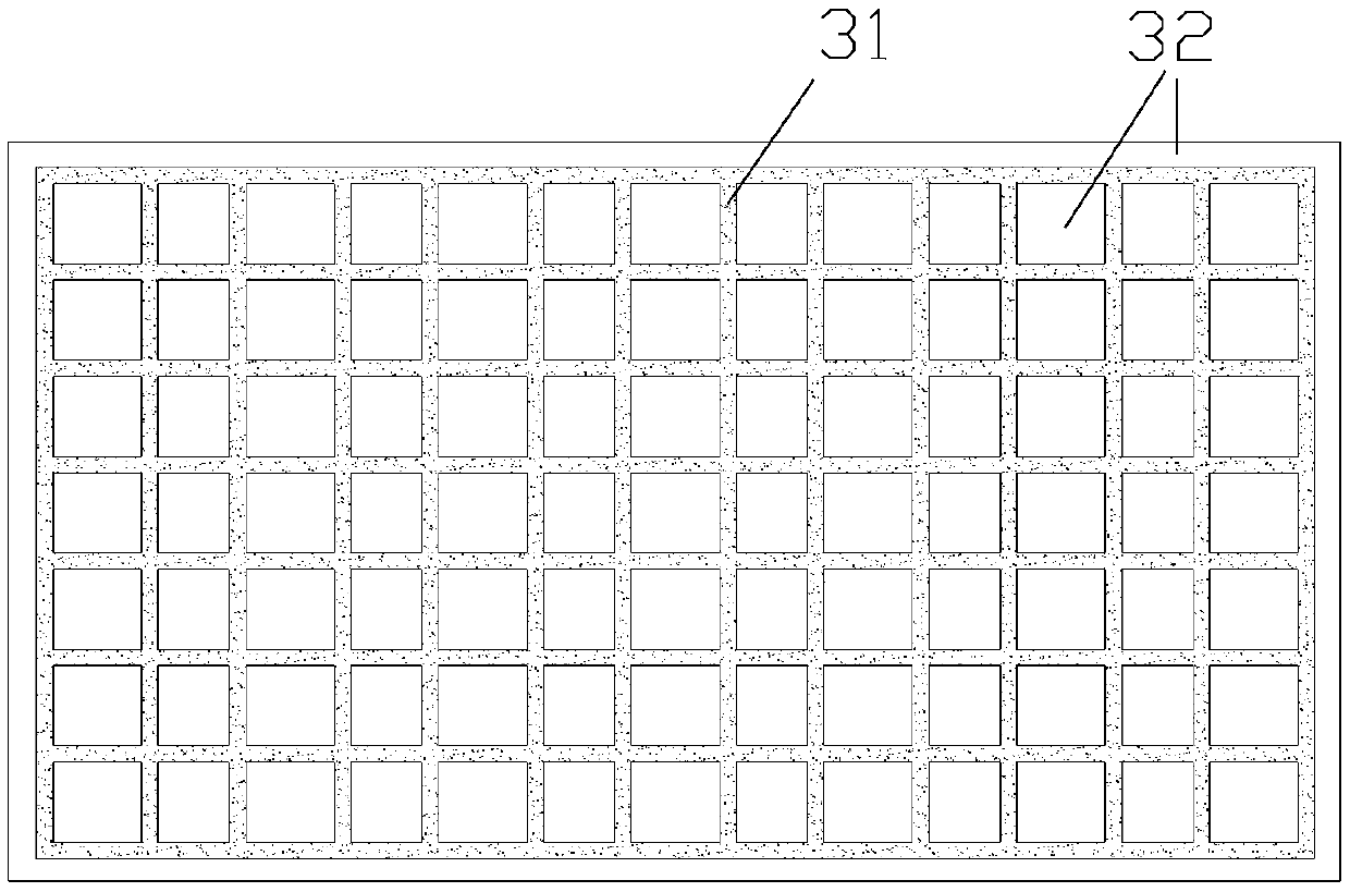
[0031] Such as Figure 1-9 As shown, the embodiment of the present invention provides an optical element, including a transparent substrate 1 , an electrochromic layer 3 and a conductive electrode 2 disposed on the transparent substrate 1 , and the conductive electrode 2 is connected to the electrochromic layer 3 . The electrochromic layer 3 includes a plurality of electrochromic lines 31 arranged at intervals on a plane parallel to the surface of the transparent substrate 1, the electrochromic lines 31 are made of electrochromic materials, and the electrochromic lines 31 are transparent when not electrified , which is translucent or opaque when...
PUM
 Abstract
Description
Claims
Application Information
 - R&D
- Intellectual Property
- Life Sciences
- Materials
- Tech Scout
- Unparalleled Data Quality
- Higher Quality Content
- 60% Fewer Hallucinations
Browse by: Latest US Patents, China's latest patents, Technical Efficacy Thesaurus, Application Domain, Technology Topic, Popular Technical Reports.
© 2025 PatSnap. All rights reserved.Legal|Privacy policy|Modern Slavery Act Transparency Statement|Sitemap|About US| Contact US: help@patsnap.com


