Display device and preparation method thereof and display device

A display device and electrode packaging technology, applied in the manufacture of semiconductor/solid-state devices, electric solid-state devices, semiconductor devices, etc., can solve the problems of low utilization rate, complex process, large film-forming area, etc., to save usage and reduce costs , the effect of improving the comprehensive mechanical properties

Active Publication Date: 2018-10-26
BOE TECH GRP CO LTD +1
View PDF5 Cites 2 Cited by
  • Summary
  • Abstract
  • Description
  • Claims
  • Application Information

AI Technical Summary

Problems solved by technology

The general OLED manufacturing process is to deposit the anode, hole injection layer, light-emitting layer, and cathode in sequence, and a diaphragm of a specific film quality must be specially set between individual pixels to separate them, and then the OLED is packaged, which is a complicated process; and the packaging material is coated. During the coating process, the film forming area is large and the utilization rate is low

Method used


Image

  • Display device and preparation method thereof and display device
  • Display device and preparation method thereof and display device
  • Display device and preparation method thereof and display device

Examples


Embodiment Construction

[0035] In order to make the purpose, technical solution and advantages of the present invention more clear, the embodiments of the present invention will be described in detail below in conjunction with the accompanying drawings. It should be noted that, in the case of no conflict, the embodiments in the present application and the features in the embodiments can be combined arbitrarily with each other.

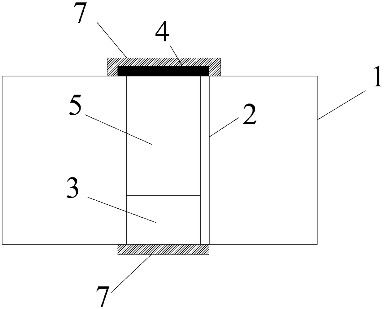
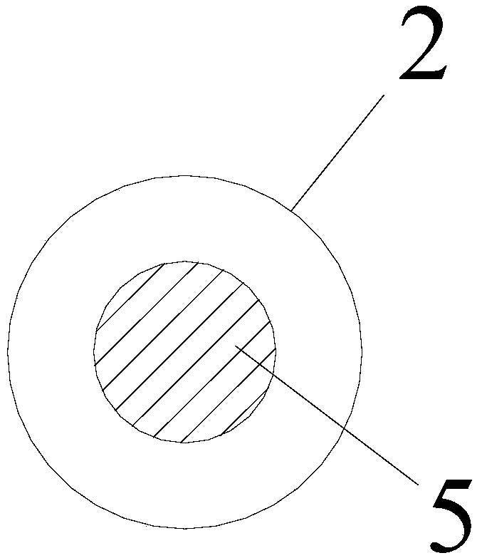
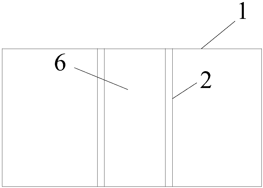
[0036] The present invention provides a display device, which includes a carrier 1, on which a nanotube 2 is arranged, and an accommodating chamber 6 with two ends open is arranged in the accommodating chamber 6, and a first An electrode 3 and a luminescent layer 5, the first electrode 3 encapsulates the opening at one end of the accommodating cavity 6, and the opening at one end of the accommodating cavity 6 away from the first electrode 3 is encapsulated by the second electrode 4, and the luminescent layer 5 Located between the first electrode 3 and the second electrode 4 ....


PUM


Abstract

The invention discloses a display device and a preparation method thereof and a display device. The display device comprises carriers which are provided with nanotubes. The nanotubes are internally provided with an accommodating cavity of which the two ends are open. A first electrode and a light-emitting layer are arranged in the accommodating cavity in a superposition way. The first electrode packages the opening of one end of the accommodating cavity. The opening of one end, which is away from the first electrode, of the accommodating cavity is packaged by the second electrode. The light-emitting layer is arranged between the first electrode and the second electrode. The display device realizes self-packaging so that the use amount of the packaging material can be saved to the greatestextent and the cost can be reduced.

Description

technical field [0001] The invention relates to the display field, in particular to a display device, a manufacturing method thereof, and a display device. Background technique [0002] Organic light-emitting diodes, that is, OLEDs, have excellent characteristics such as ultra-thin, low power consumption, fast response speed, self-illumination, high contrast, wide viewing angle, and can be used for flexible panels. The general OLED manufacturing process is to deposit the anode, hole injection layer, light-emitting layer, and cathode in sequence, and a diaphragm of a specific film quality must be specially set between individual pixels to separate them, and then the OLED is packaged, which is a complicated process; and the packaging material is coated. During the covering process, the film forming area is large and the utilization rate is low. Contents of the invention [0003] In order to solve the above technical problems, the present invention provides a display device,...

Claims


Application Information

Patent Timeline
Patent Type & Authority Applications(China)
IPC IPC(8): H01L51/52H01L51/56B82Y30/00
CPCB82Y30/00H10K50/805H10K50/841H10K71/00H10K50/80H10K50/182H10K2102/3023H10K50/84
Inventor 董晓楠谌伟吴旭黄中浩赵永亮
Owner BOE TECH GRP CO LTD
Why Eureka
Try Eureka