A semiconductor diode pin forming device

A molding device and diode technology, applied in semiconductor/solid-state device manufacturing, electrical components, circuits, etc., can solve problems such as pin scratches, quality problems, and positioning groove dust that cannot be cleaned in time

Active Publication Date: 2020-11-10
滨州高新高端装备制造产业园有限公司
View PDF7 Cites 0 Cited by
  • Summary
  • Abstract
  • Description
  • Claims
  • Application Information

AI Technical Summary

Problems solved by technology

However, in this solution, the pins rub against the lower mold during bending, which leads to scratches on the pins, which in turn leads to quality problems; the bending angle of the pins cannot be adjusted, and the bending fillet of the pins cannot be adjusted, which leads to the inapplicability of the product. Low stability; the dust in the positioning groove cannot be cleaned in time after bending

Method used


Image

  • A semiconductor diode pin forming device
  • A semiconductor diode pin forming device
  • A semiconductor diode pin forming device

Examples


Embodiment approach

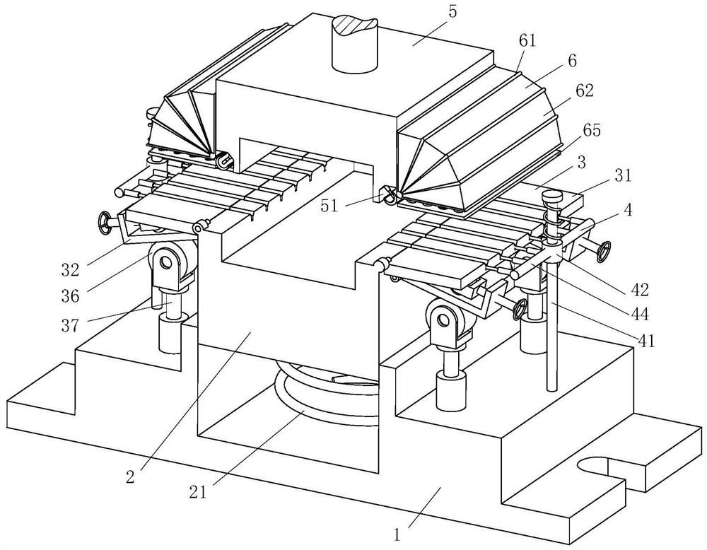
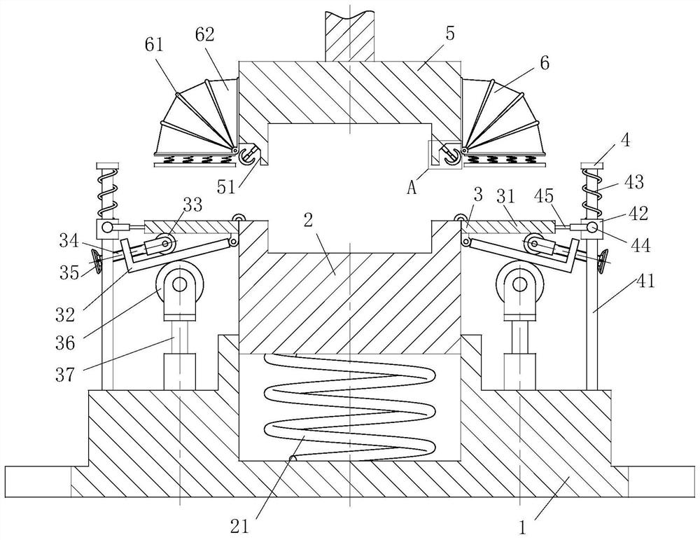
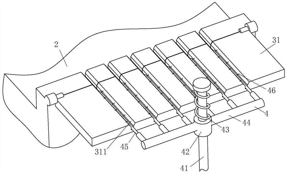
[0024]As an embodiment of the present invention, the bending module 3 includes a positioning plate 31, an adjusting plate 32, a No. 1 roller 33, an adjusting screw 34, a hand wheel 35, a No. 2 roller 36, and an electric cylinder 37. The positioning plate One end of 31 is hinged to the edge of the top side of lower die 2; the top surface of the positioning plate 31 is provided with a group of No. 1 positioning grooves 311, and the bottom surface of one end of the positioning plate 31 is hinged to one end of the adjusting plate 32; the adjusting plate 32 is L-shaped; The adjusting screw 34 is connected with the adjusting plate 32 by threads; one end of the adjusting screw 34 is fixedly connected with the handwheel 35, and the other end of the adjusting screw 34 is connected with the No. 1 roller 33 through a rotating shaft; Between 32, the No. 1 roller 33 is driven by the adjusting screw 34 to realize the adjustment of the angle between the positioning plate 31 and the adjusting ...


PUM


Abstract

The invention belongs to the technical field of semiconductor diode manufacturing, in particular to a semiconductor diode pin forming device. The semiconductor diode pin forming device comprises a fixed base, a lower die, a bending module, a dust removal module, an upper die and a compressing module; the lower die is slidably connected in a cavity in the top of the fixed base; the bending module is hinged to the two sides of the top of the lower die, and the dust removal module is arranged on the non-hinged side of the bending module; the bottom of the dust removal module is fixedly connectedto the step surface of the fixed base; the upper die is arranged above the lower die; the top of the upper die is fixedly connected with the output end of a crimping machine; and the two sides of theupper die are fixedly connected with the compressing module. According to the semiconductor diode pin forming device, the bending module is hinged to the two sides of the top of the lower die, so thatwhen the lower die moves downwards, the bending module swings around the hinged position to realize pin bending; meanwhile, the bending angle of the bending module can be adjusted; and the dust removal module is arranged on the non-hinged side of the bending module, so that dust in the number one positioning groove of the bending module can be removed.

Description

technical field [0001] The invention belongs to the technical field of semiconductor diode manufacturing, in particular to a semiconductor diode pin forming device. Background technique [0002] Diode bending foot forming process is already a relatively mature process in the market, and there are also various automation equipment, which can solve the forming process of product diversification. But the disadvantages are also obvious. It is suitable for products with large quantities and few varieties, and it must be a braided product. There are also limitations on the thickness of the pins, and it cannot be popularized to all products. And the equipment cost is also high, it is impossible to standardize and automate the production of all products used. Usually, for small-batch products and repairs and supplements, most of them are carried out by manual bending. This method is difficult to guarantee dimensional accuracy, affects product quality, and is inefficient and labor-i...

Claims


Application Information

Patent Timeline
Patent Type & Authority Patents(China)
IPC IPC(8): H01L21/02H01L21/48H01L21/67
CPCH01L21/02057H01L21/02096H01L21/4896H01L21/67253
Inventor 陈欣洁王勇
Owner 滨州高新高端装备制造产业园有限公司
Why Eureka
Try Eureka