Chip data self-destruction package structure
A technology of packaging structure and data, applied in electrical components, electrical solid devices, circuits, etc., can solve the problems of no packaging-level disassembly to propose defense methods, increase the complexity of data reading, and cannot block data reading.
- Summary
- Abstract
- Description
- Claims
- Application Information
AI Technical Summary
Problems solved by technology
Method used
Image

Examples
Embodiment 1
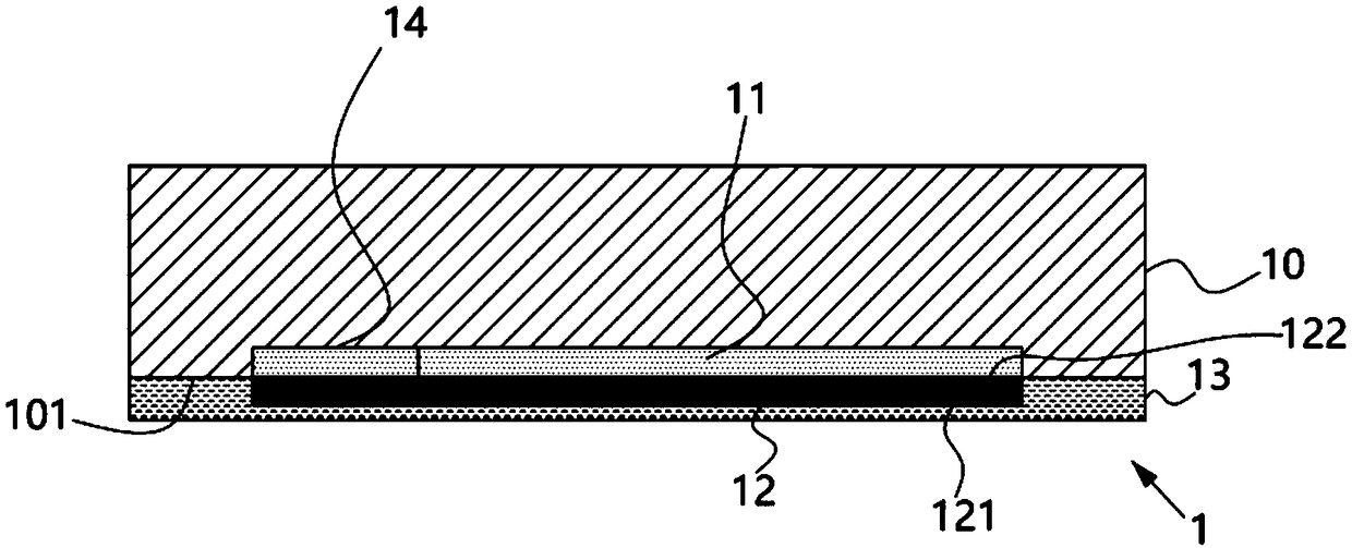
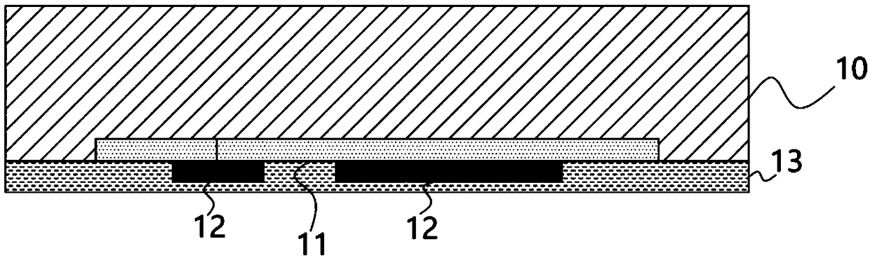
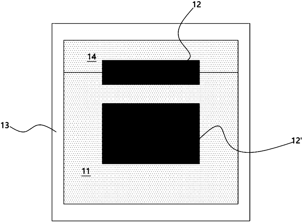
[0028] refer to figure 1 The shown chip data self-destruct packaging structure 1 includes a storage unit 10, the storage unit includes a thermal failure memory 11 that automatically erases data at a temperature higher than a certain temperature and a control circuit 14 that is electrically connected to the thermal failure memory 11; The heat generated during the decomposition process is conducted to the heat conductor 12 of the thermal failure memory 11 and the chemical protection layer 13 attached to the heat conductor 12 and the surface of the storage unit.
[0029] According to the above technical solution, the heat generated when the chip package structure 1 is disassembled heats the thermal conductor 12, and after the thermal conductor 12 is heated, it transfers the heat to the thermal failure memory 11, and the thermal failure memory 11 is heated to a certain threshold Automatically erase data.
[0030] The heat conductor 12 includes a heat absorbing area 121 and a heat...
Embodiment 2
[0041] refer to Figure 6 The bottom of the chip packaging structure is provided with a metal layer 17, the metal layer 17 is an electrode connecting the thermal failure memory 11 and the control circuit 14, and the electrode is connected to the PCB board at the bottom or the bottom of the chip packaging structure through the solder 18 layer. The substrate 19 is connected, and the electrode 17 is a copper column arranged at the bottom 14 of the thermal failure memory 11 and the control circuit; the heat absorption area 171 of the electrode 17 is connected to the solder layer at the bottom of the electrode, and the solder layer 18 is used when the chip is disassembled and packaged. The heat at the bottom is conducted to the thermal failure memory through the bottom heat absorption area 171 and the upper heat dissipation area 172 .
[0042] In a simpler implementation, solder 18 can be directly used to connect the thermal failure memory 11 and the substrate 19 at the bottom, the...
Embodiment 3
[0044] refer to Figure 7 , presents the third chip anti-static analysis structure solution, the chip packaging structure includes a substrate 15 . The substrate 15 includes a bearing surface 151 and an electrical connection surface 152. A solder ball 16 is arranged on the electrical connection surface 152 of the substrate. The solder ball 16 serves to fix the substrate 15 and the storage unit 10 while the solder ball is also used as a heat conductor. The heat dissipation area 161 is above the solder ball 16 in the height direction, and the heat absorption area 162 is below the solder height direction. The heat dissipation area 162 is connected to the carrying surface 151 of the substrate. It should be noted that the heat dissipation area 162 and the position of the heat dissipation area 162 are related to the heated area of the solder ball 16 when the chip package structure is thermally disassembled.
[0045] In this solution, the thermal conductor is a discrete solder ba...
PUM
 Abstract
Description
Claims
Application Information
 - R&D
- Intellectual Property
- Life Sciences
- Materials
- Tech Scout
- Unparalleled Data Quality
- Higher Quality Content
- 60% Fewer Hallucinations
Browse by: Latest US Patents, China's latest patents, Technical Efficacy Thesaurus, Application Domain, Technology Topic, Popular Technical Reports.
© 2025 PatSnap. All rights reserved.Legal|Privacy policy|Modern Slavery Act Transparency Statement|Sitemap|About US| Contact US: help@patsnap.com