Mirror surface display screen and preparation method
A technology for display screens and opening areas, which is applied in semiconductor/solid-state device manufacturing, organic semiconductor devices, semiconductor devices, etc., and can solve problems such as large resistance, uneven screen brightness, and high power consumption of OLED displays
- Summary
- Abstract
- Description
- Claims
- Application Information
AI Technical Summary
Problems solved by technology
Method used
Image


Examples
Embodiment Construction
[0033] The following will clearly and completely describe the technical solutions in the embodiments of the present invention with reference to the accompanying drawings in the embodiments of the present invention. Obviously, the described embodiments are only some, not all, embodiments of the present invention. Based on the embodiments of the present invention, all other embodiments obtained by persons of ordinary skill in the art without making creative efforts belong to the protection scope of the present invention.
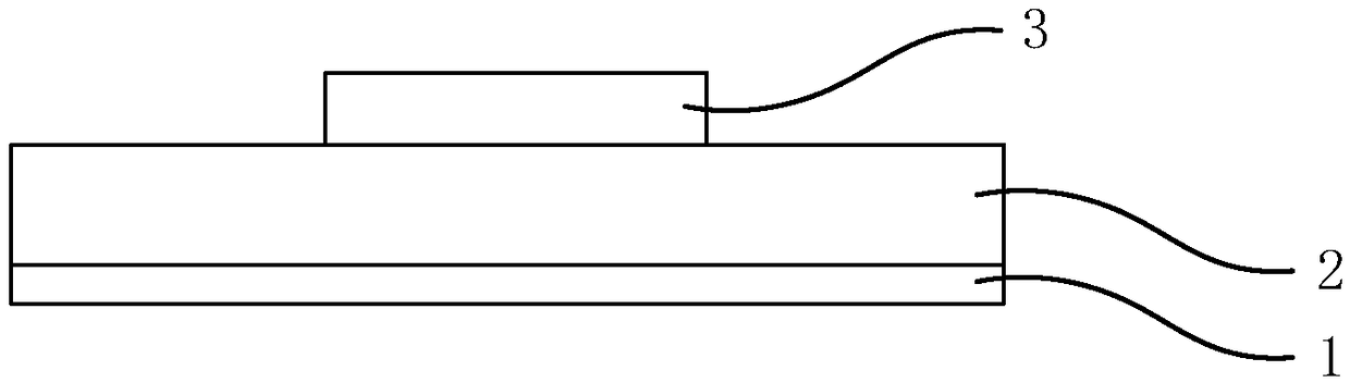
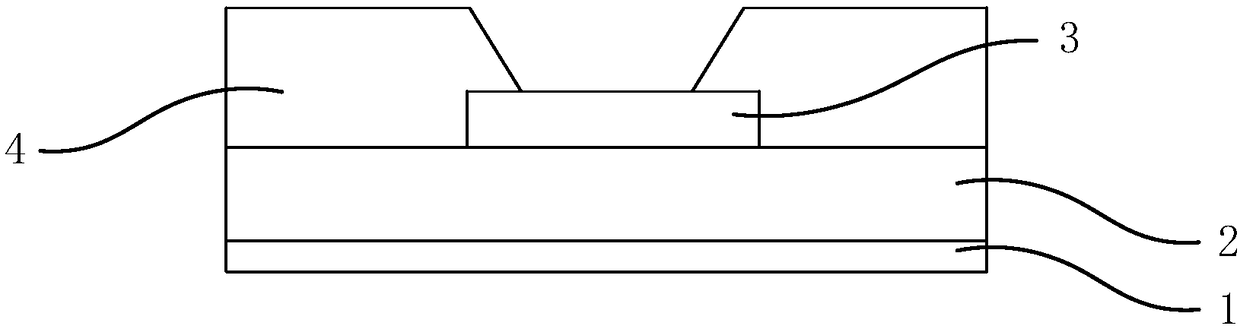
[0034] Please refer to Figure 5 , Figure 10 and Figure 15 , the present invention provides a mirror display screen, comprising:
[0035] substrate substrate 1;
[0036] A flat layer 2 disposed on one side of the base substrate 1;
[0037] The pixel defining layer 4 disposed on the side of the flat layer 2 facing away from the base substrate 1, the pixel defining layer 4 is formed with a plurality of opening regions distributed in an array;
[0038] An ...
PUM
 Abstract
Description
Claims
Application Information
 - R&D
- Intellectual Property
- Life Sciences
- Materials
- Tech Scout
- Unparalleled Data Quality
- Higher Quality Content
- 60% Fewer Hallucinations
Browse by: Latest US Patents, China's latest patents, Technical Efficacy Thesaurus, Application Domain, Technology Topic, Popular Technical Reports.
© 2025 PatSnap. All rights reserved.Legal|Privacy policy|Modern Slavery Act Transparency Statement|Sitemap|About US| Contact US: help@patsnap.com