Pixel substrate, liquid crystal display panel and liquid crystal display

A liquid crystal display and substrate technology, applied in static indicators, instruments, nonlinear optics, etc., can solve problems affecting the display effect and impact of liquid crystal displays

Inactive Publication Date: 2018-11-09
WUHAN CHINA STAR OPTOELECTRONICS TECH CO LTD
View PDF5 Cites 1 Cited by
  • Summary
  • Abstract
  • Description
  • Claims
  • Application Information

AI Technical Summary

Problems solved by technology

[0005] This application mainly provides a pixel substrate, a liquid crystal display panel and a liquid crystal display, which are used to solve the problem that different feedthrough voltages will affect the voltage of the common electrode when the driving method of reducing power consumption is adopted, thereby affecting the display effect of the liquid crystal display

Method used


Image

  • Pixel substrate, liquid crystal display panel and liquid crystal display
  • Pixel substrate, liquid crystal display panel and liquid crystal display
  • Pixel substrate, liquid crystal display panel and liquid crystal display

Examples


Embodiment Construction

[0024] The following will clearly and completely describe the technical solutions in the embodiments of the application with reference to the drawings in the embodiments of the application. Apparently, the described embodiments are only some of the embodiments of the application, not all of them. Based on the embodiments in this application, all other embodiments obtained by persons of ordinary skill in the art without making creative efforts belong to the scope of protection of this application.

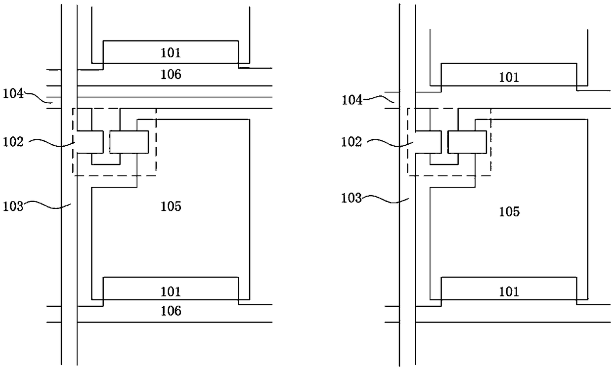
[0025] This application provides a pixel substrate, see figure 1 , figure 1 It is a schematic structural diagram of an embodiment of the pixel substrate in this application, such as figure 1 The pixel substrate shown includes: a TFT 102, a source line 103, a gate line 104, a liquid crystal pixel 105, a common electrode 106 and a corresponding storage capacitor 101, wherein the TFT 102 is arranged between the source line 103, the gate line 104 and the liquid crystal pixel 105 , ...


PUM


Abstract

The invention discloses a pixel substrate, a liquid crystal display panel and a liquid crystal display. The pixel substrate comprises a liquid crystal pixel, TFTs, source lines, gate lines, a common electrode and corresponding storage capacitors; the liquid crystal pixel comprises a plurality of pixel units, each source line is connected with the source / drain electrodes of at least two columns ofpixel units, and the value of the storage capacitor corresponding to one column of pixel units is larger than that of the storage capacitors corresponding to the other columns of pixel units. The influence of the feed-through effect on the display effect is reduced while the power consumption is reduced.

Description

technical field [0001] The present application relates to the field of display technology, in particular to a pixel substrate, a liquid crystal display panel and a liquid crystal display. Background technique [0002] With the rapid development of TFT-LCD liquid crystal technology, people's requirements for the clarity of LCD display are getting higher and higher, that is, the resolution of liquid crystal display is getting higher and higher; the increase of resolution requires the source of the output of the source integrated circuit The more lines there are. At present, the general technical solution is to separately charge the sub-pixels through MUX switching and time-division multiplexing, so as to achieve the purpose of reducing the number of output source lines of the source integrated circuit. [0003] In the prior art, the TFT-LCD liquid crystal panel generally adopts the Demux drive architecture, such as figure 2 and image 3 as shown, figure 2 It is a structura...

Claims


Application Information

Patent Timeline
Patent Type & Authority Applications(China)
IPC IPC(8): G02F1/133G02F1/1362
CPCG02F1/13306G02F1/136213G02F1/136286
Inventor 左清成
Owner WUHAN CHINA STAR OPTOELECTRONICS TECH CO LTD
Why Eureka
Try Eureka