IC design circuit board debugging system of LED lamp and debugging method

A technology of LED lighting and debugging system, which is applied in the direction of electronic circuit testing, measuring electricity, measuring electrical variables, etc., can solve the problems of labor cost increase, unguaranteed detection rate, missed detection and wrong judgment, etc., so as to reduce the time spent, The debugging process is simple and convenient, and the effect of improving efficiency and accuracy

Inactive Publication Date: 2018-11-13
ANHUI SHILIN LIGHTING
View PDF8 Cites 0 Cited by
  • Summary
  • Abstract
  • Description
  • Claims
  • Application Information

AI Technical Summary

Problems solved by technology

[0002] At present, when debugging the IC design circuit of LED lamps, most of them are debugged manually. Manual detection is usually by manually outputting a detection signal to the circuit board, and then comparing whether the output signal of the circuit board is consistent with the correct output signal. However, at present, manual detection of the circuit board In between, the components on the surface of the circuit board must be inspected. This process is a test of the staff's eyesight. Long-term inspection will easily cause eye fatigue of the inspectors, resulting in missed inspections and misjudgments. The detection rate cannot be guaranteed. When the position of the components is not correct When the detection signal is output to the circuit board, it is easy to cause damage to the components of the circuit board. If it is provided to customers, it has to rely on increasing the number of inspectors to ensure the speed of inspection, which will lead to a substantial increase in labor costs

Method used


Image

  • IC design circuit board debugging system of LED lamp and debugging method
  • IC design circuit board debugging system of LED lamp and debugging method

Examples


Embodiment Construction

[0036] The preferred embodiments of the present invention will be described in detail below in conjunction with the accompanying drawings, so that the advantages and features of the present invention can be more easily understood by those skilled in the art, so as to define the protection scope of the present invention more clearly.

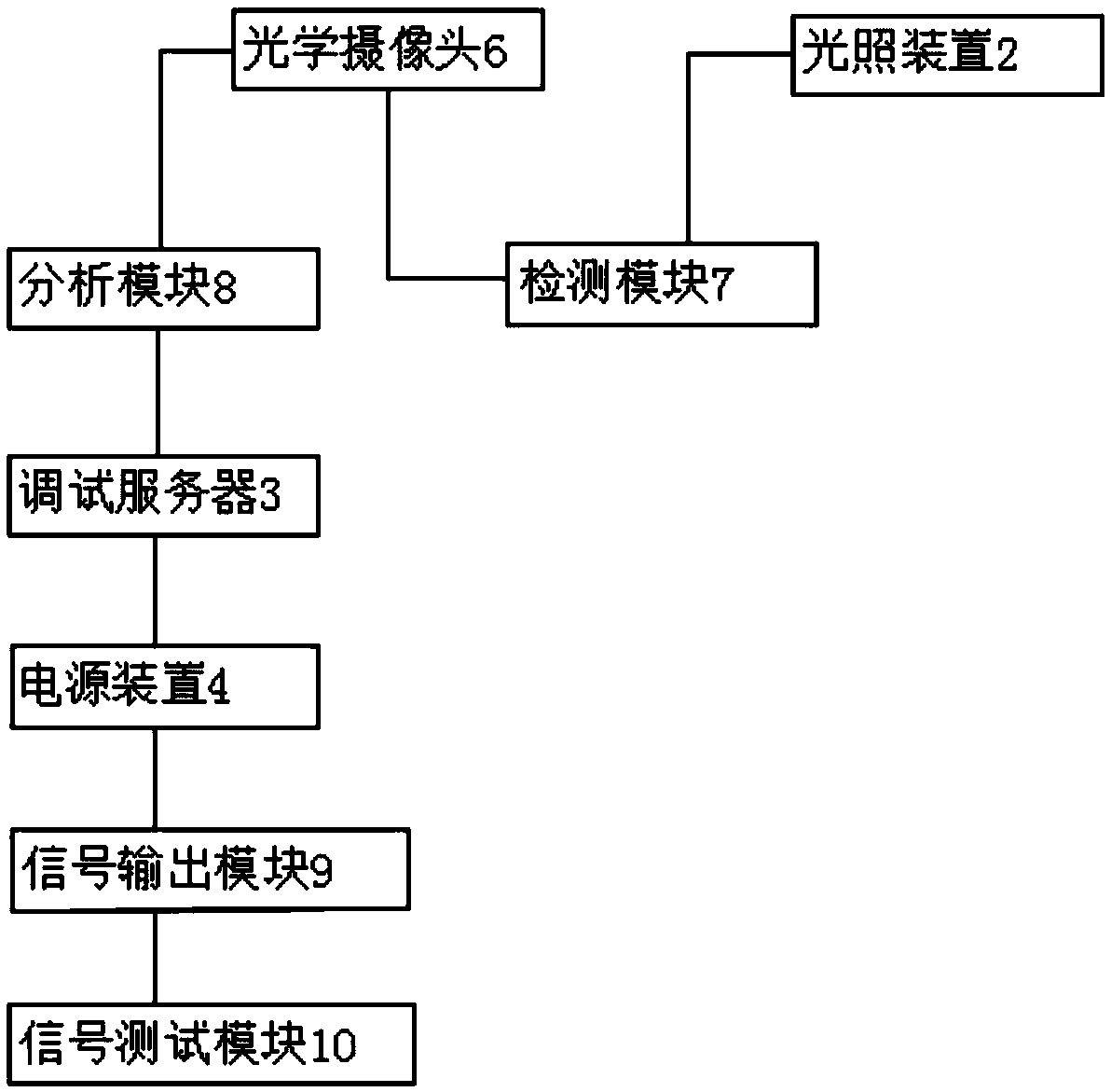
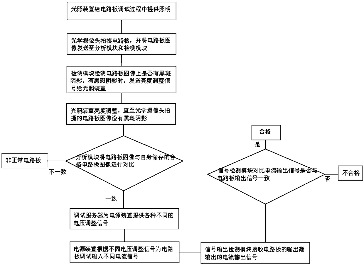
[0037] refer to figure 1 and figure 2 As shown, the present invention provides a LED lamp IC design circuit board debugging system, including the following components:

[0038] The optical imaging device 1 is used to collect the optical image of the circuit circuit on the surface of the circuit board, and analyze whether the circuit board is qualified;

[0039] The lighting device 2 is used to provide lighting for the circuit board debugging process, and the lighting brightness can be adjusted according to the optical image of the circuit line;

[0040] The debugging server 3 is used to provide various voltage adjustment signals for the power ...


PUM


Abstract

The invention discloses an IC design circuit board debugging system of an LED lamp and a debugging method. An optical imaging device is used for collecting an optical image of a circuit board surfacecircuit line. An illuminating device is used for providing illumination in a circuit board debugging process. A debugging server is used for providing different voltage adjustment signals for a powersource device. The power source device is used for receiving the different voltage adjustment signals sent by the debugging server. A detecting device is used for detecting a current signal output inthe circuit board debugging process, and detecting whether a circuit board is qualified according to the output current signal. Firstly, the system is capable of detecting whether a position of an element on the surface of the circuit board is correct or not, and a problem that the element is mis-plugged on the circuit board is avoided. While the position of the element is correct, the circuit board is debugged through a detection signal, the debugging efficiency and accuracy of the circuit board are greatly improved, a debugging process is simple and convenient, and spent time of artificiallydebugging the circuit board is reduced at the same time.

Description

technical field [0001] The invention relates to the technical field of circuit board debugging, and more specifically relates to a debugging system and a debugging method for an IC design circuit board of an LED lamp. Background technique [0002] At present, when debugging the IC design circuit of LED lamps, most of them are debugged manually. Manual detection is usually by manually outputting a detection signal to the circuit board, and then comparing whether the output signal of the circuit board is consistent with the correct output signal. However, at present, manual detection of the circuit board In between, the components on the surface of the circuit board must be inspected. This process is a test of the staff's eyesight. Long-term inspection will easily cause eye fatigue of the inspectors, resulting in missed inspections and misjudgments. The detection rate cannot be guaranteed. When the position of the components is not correct When the detection signal is output t...

Claims


Application Information

Patent Timeline
IPC IPC(8): G01N21/956G01R31/28
CPCG01N21/956G01N2021/95638G01R31/2806
Inventor 仇怀利桑永树李运鹤刘军
Owner ANHUI SHILIN LIGHTING
Why Eureka
Try Eureka