Display panel and display device

A technology of display panel and encapsulation layer, which is applied in the manufacturing of electrical components, electric solid-state devices, semiconductor/solid-state devices, etc., can solve the problems of large light-emitting thickness, poor viewing angle of OLED devices, and prone to cross-coloring of pixels.

Inactive Publication Date: 2018-11-13
BOE TECH GRP CO LTD
View PDF6 Cites 12 Cited by
  • Summary
  • Abstract
  • Description
  • Claims
  • Application Information

AI Technical Summary

Problems solved by technology

[0004] Embodiments of the present invention provide a display panel and a display device, which are used to solve the problem in the prior art that the OLE

Method used


Image

  • Display panel and display device
  • Display panel and display device
  • Display panel and display device

Examples


Embodiment Construction

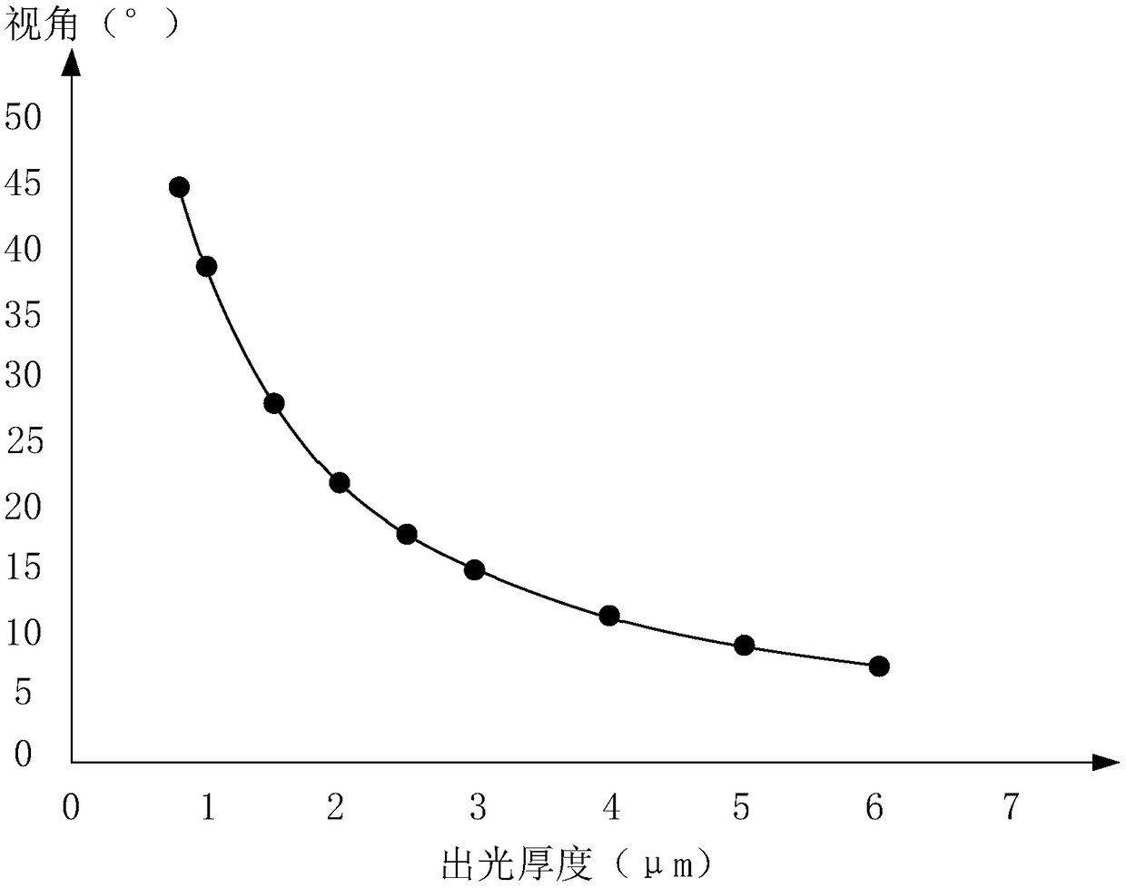
[0037] Aiming at the problem in the prior art that the light emitting thickness of the OLED device is relatively large, color crossover between pixels is prone to occur, resulting in a poor viewing angle of the OLED device, the embodiments of the present invention provide a display panel and a display device.

[0038] The specific implementation manners of the display panel and the display device provided by the embodiments of the present invention will be described in detail below with reference to the accompanying drawings. The thickness and shape of each film layer in the drawings do not reflect the real scale, and the purpose is only to illustrate the content of the present invention.

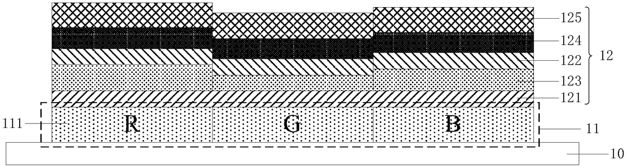
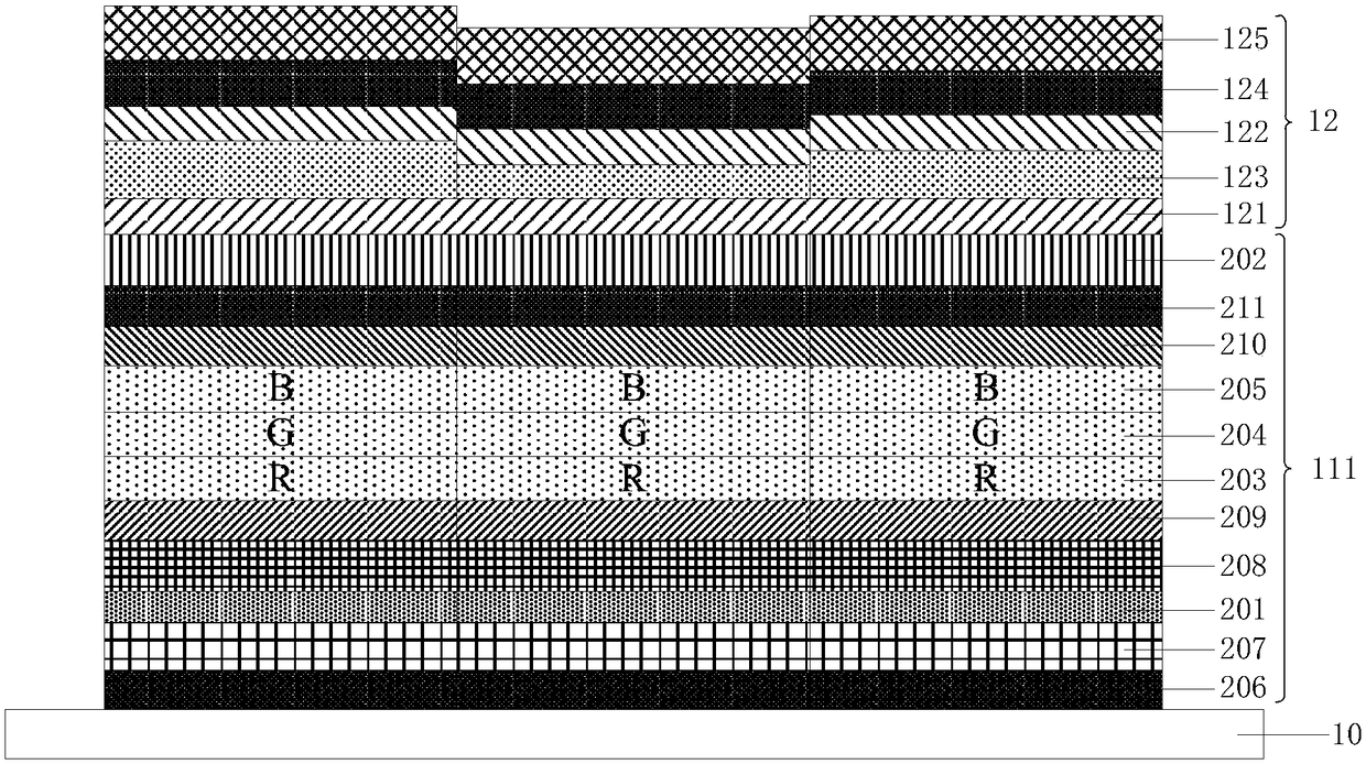
[0039] In a first aspect, an embodiment of the present invention provides a display panel, such as figure 2 As shown, it includes: a base substrate 10, a plurality of pixel units 11 located on the base substrate 10, each pixel unit 11 includes a plurality of sub-pixel units 111, and a pack...


PUM

PropertyMeasurementUnit
Thicknessaaaaaaaaaa
Thicknessaaaaaaaaaa
Thicknessaaaaaaaaaa

Abstract

The invention discloses a display panel and a display device. The display panel comprises a substrate, pixel units positioned on the substrate and an encapsulation layer, each pixel unit comprises multiple sub-pixel units, and the encapsulation layer covers the sub-pixel units and has a filtering function; the encapsulation layer comprises a first reflection layer, a second reflection layer, a dielectric layer and at least one inorganic layer; the different sub-pixel units in the pixel unit correspond to different thicknesses of dielectric layers in the encapsulation layer; and the dielectriclayer, the first reflection layer and the second reflection layer corresponding to the same sub-pixel unit form a micro cavity structure, the micro cavity structure allows light corresponding to colorof the sub-pixel unit to pass and does not light of other color to pass, thus, the filtering function is realized. The encapsulation layer has functions of encapsulation and filtering, so that it isnot required to set colored optical filters, the thickness of outlet light is reduced, cross-color phenomena can be reduced among the pixels, a visual angle of the display panel is increased, and a product is more competitive.

Description

technical field [0001] The invention relates to the field of display technology, in particular to a display panel and a display device. Background technique [0002] Organic Light Emitting Display (OLED) refers to a phenomenon in which organic semiconductor materials and luminescent materials are driven by an electric field to cause light emission through carrier injection and recombination. OLED devices have attracted the attention of the market for their unique advantages. For example, OLED devices have active light emission, full curing, no viewing angle problems, light weight, small thickness, high brightness, high luminous efficiency, fast response speed, and high dynamic picture quality. It has a wide temperature range, flexible display, simple process, low cost, and strong shock resistance. In addition, the application of OLED devices is also very diversified, such as flexible, transparent and micro-displays, etc., all have OLED devices. [0003] At present, OLED de...

Claims


Application Information

Patent Timeline
IPC IPC(8): H01L51/52H01L27/32
CPCH10K59/00H10K50/84H10K50/852
Inventor 王灿张粲岳晗杨明丛宁玄明花
Owner BOE TECH GRP CO LTD
Why Eureka
Try Eureka