

PCB composite board for PTC heater
A combination board and heater technology, applied in battery pack parts, conductive connections, electrical components, etc., can solve the problems of unsafe use of high and low voltage electrodes, electromagnetic interference of PCB circuit boards, and low heat dissipation performance, and achieve easy heat dissipation, The effect of eliminating false welding and improving safety
- Summary
- Abstract
- Description
- Claims
- Application Information
AI Technical Summary
Problems solved by technology
Method used
Image

Examples
Embodiment 1
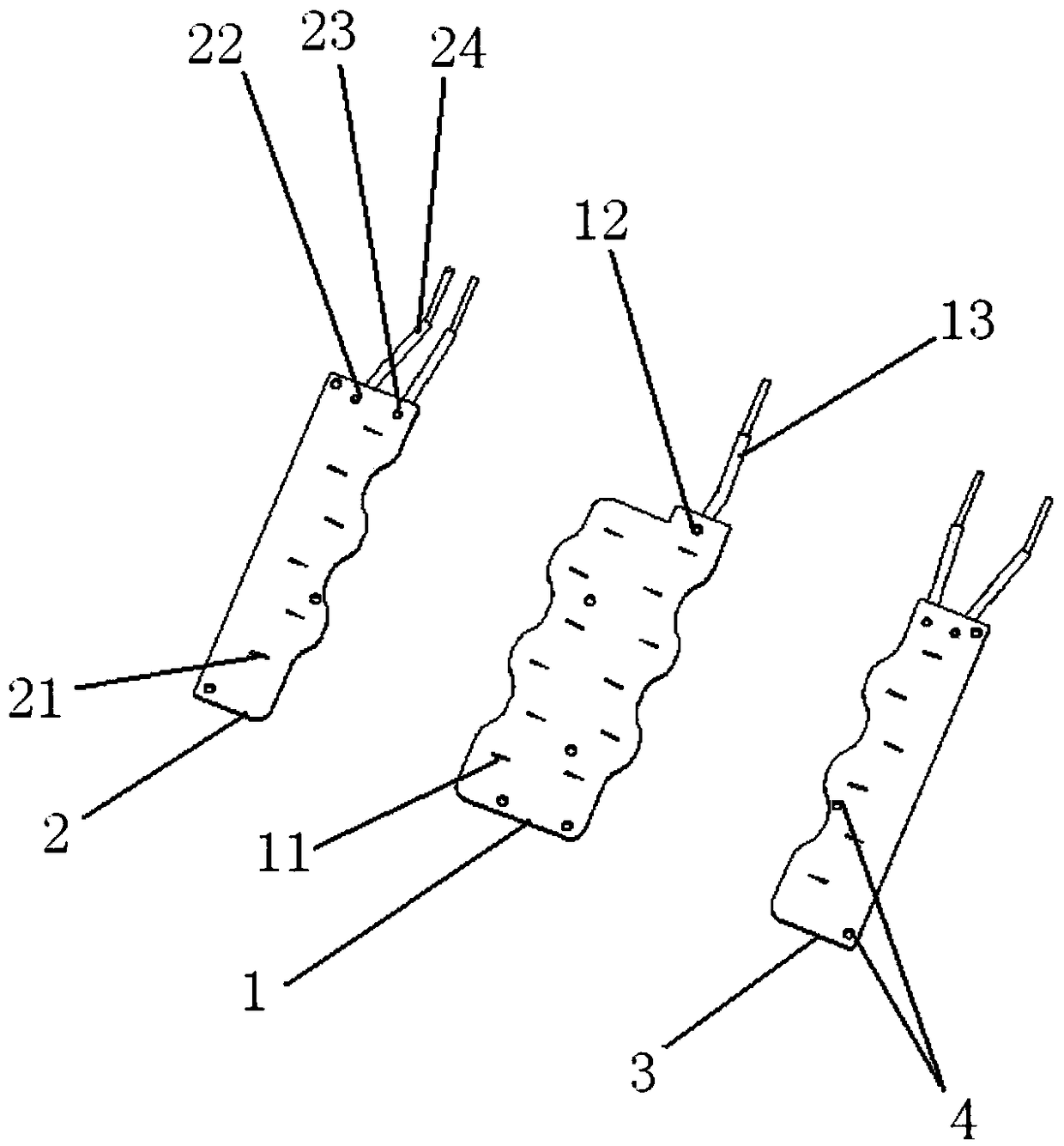
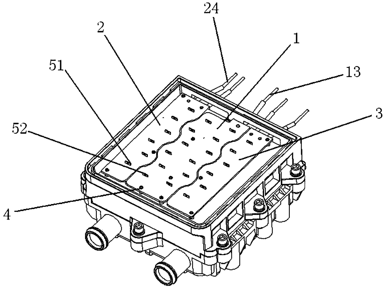
[0016] Embodiment 1 discloses a PCB combination board for a PTC heater, such as figure 1 As shown, it includes a positive plate 2, two negative plates 2 and a negative plate 3, two rows of positive plate jacks 11 are provided on the positive plate 2, and a row of negative plate jacks 21 are provided on the negative plate 2 and the negative plate 3. The end of the positive plate 2 is also provided with a positive line welding end (pad) 12, and the end of the negative plate 2 is provided with a negative line welding end (pad) 22 and a negative line welding end (pad) 23; The welding end 12 is electrically connected to the positive electrode socket 11 through the positive printed circuit (not marked in the figure) on the positive plate 1; The negative electrode printed circuit (not marked) on the negative electrode plate 2 and the negative electrode plate 3 is electrically connected; the positive electrode plate 1 and the negative electrode plate 2 or the negative electrode plate ...
Embodiment 2
[0019] Embodiment 2 discloses a PCB combination board for a PTC heater, comprising a positive plate 2, two negative plates 2 and a negative plate 3, two rows of positive plate jacks 11 are provided on the positive plate 2, the negative plate 2 and the negative plate 3 are provided with a row of negative plate jacks 21; the end of the positive plate 2 is also provided with a positive line welding end (pad) 12, and the end of the negative plate 2 is provided with a negative line welding end (pad) 22 and negative electrode Wire welding end (pad) 23; positive wire welding end 12 and positive electrode sheet jack 11 are electrically connected through the positive electrode printed circuit (not marked in the figure) on positive electrode plate 1; negative electrode wire welding end 22 and negative electrode wire welding The terminal 23 is electrically connected to the negative plate jack 21 respectively through the negative printed circuit (not marked in the figure) on the negative p...
Embodiment 3
[0022] The connection and position of the components in this embodiment are the same as those in Embodiment 2. The only difference is that the PCB combination board in this embodiment is composed of 5 pieces of spliced boards, and the arrangement is negative plate, positive plate from left to right. plate, negative plate, positive plate and negative plate; wherein the positive plate is provided with two rows of positive plate jacks 11, the negative plate in the middle is also provided with two rows of negative plate jacks 21, and the negative plates on both sides are provided with There is a row of negative plate jacks 21; the installation method is the same as that in Embodiment 2.
PUM
 Abstract
Description
Claims
Application Information