Array substrate, display panel and display device

An array substrate and display area technology, applied in static indicators, instruments, nonlinear optics, etc., can solve problems such as frame width, and achieve the effect of reducing the area, being conducive to narrowing the frame, and reducing the space occupied

Active Publication Date: 2018-11-23
SHANGHAI AVIC OPTOELECTRONICS
View PDF7 Cites 9 Cited by
  • Summary
  • Abstract
  • Description
  • Claims
  • Application Information

AI Technical Summary

Problems solved by technology

[0005] The object of the present invention is to provide an array substrate, a display panel and a display device including the same, so as to solve the problem of wider borders caused by the existence of dummy shift registers

Method used


Image

  • Array substrate, display panel and display device
  • Array substrate, display panel and display device
  • Array substrate, display panel and display device

Examples


Embodiment Construction

[0026] The present invention will be further described in detail below in conjunction with the accompanying drawings and embodiments. It should be understood that the specific embodiments described here are only used to explain the present invention, but not to limit the present invention. In addition, it should be noted that, for the convenience of description, only some structures related to the present invention are shown in the drawings but not all structures.

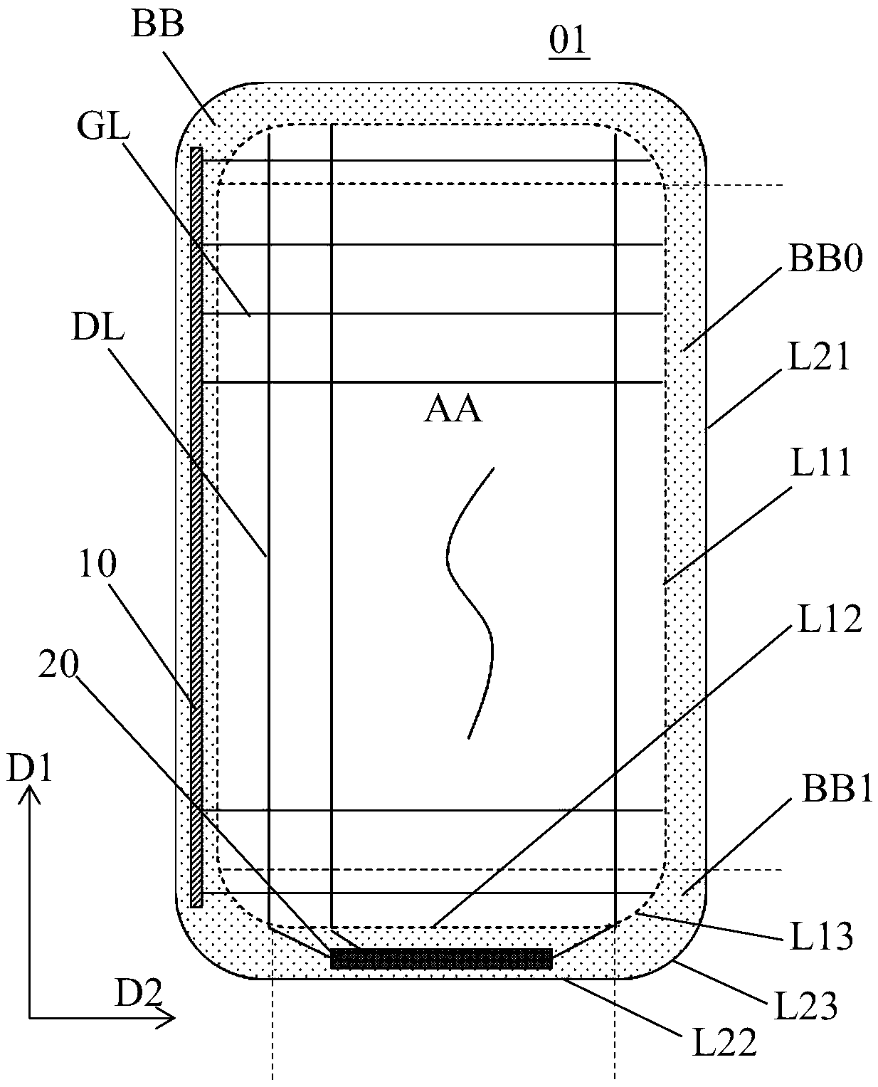
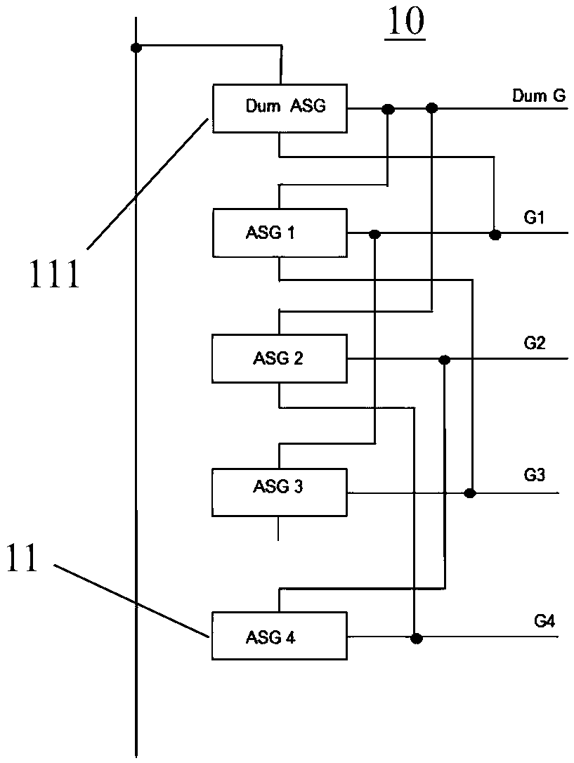
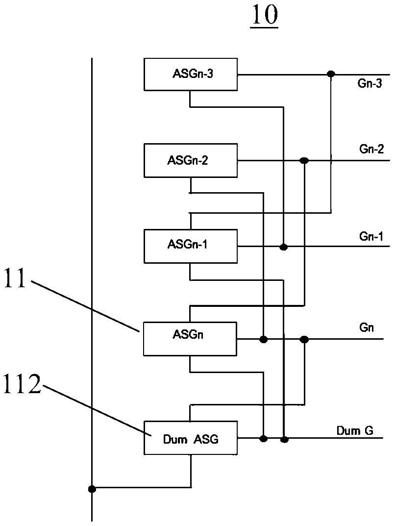
[0027] The invention discloses an array substrate, comprising a display area and a non-display area surrounding the display area, the non-display area includes a non-display area with a special shape, located between the special-shaped boundary of the display area and the special-shaped edge of the array substrate space; the dummy scan lines of the array substrate are located in the non-display area of ​​the special shape, which can reduce the occupied space of the dummy scan lines in the non-display area, reduce t...


PUM


Abstract

The invention discloses an array substrate, a display panel and a display device. The array substrate comprises a display area and a non-display area surrounding the display area, the non-display areacomprises an abnormal non-display area, wherein the abnormal non-display area is located between the abnormal boundary of the display area and the abnormal edge of the array substrate; a dummy scanning line of the array substrate is located in the abnormal non-display area, can reduce space occupied by the dummy scanning line in the non-display area, reduces the area of the non-display area of the array substrate, and is conductive to the narrow bezel of the display device.

Description

technical field [0001] The present invention relates to the field of display technology, and in particular to an array substrate, a display panel and a display device including the same. Background technique [0002] In a conventional display device, the display panel is mostly a rectangular structure. However, with the continuous development of display technology and the diversified demands of users on the appearance of display devices, special-shaped display panels have been more and more widely used. [0003] Taking the liquid crystal display panel as an example, the liquid crystal display panel and the liquid crystal display device are one of the current mainstream display technologies. The liquid crystal display panel includes a plurality of pixel units, and each pixel unit includes insulated and crossed scanning lines, data lines and thin film transistors. Wherein, the data line receives the data signal, controls the driving voltage of each sub-pixel, thereby controls...

Claims


Application Information

Patent Timeline
Patent Type & Authority Applications(China)
IPC IPC(8): G02F1/1362G02F1/1345G09G3/36
CPCG02F1/13454G02F1/136286G09G3/3677
Inventor 金慧俊
Owner SHANGHAI AVIC OPTOELECTRONICS
Why Eureka
Try Eureka