
A kind of inorganic non-lead cesium bismuth halide cs 3 bi 2 x 9 Perovskite microdisk and its synthesis method

A synthetic method and inorganic non-technique, applied in the direction of bismuth compounds, inorganic chemistry, chemical instruments and methods, etc., can solve the problems of narrow synthesis window and difficulty in the synthesis of micron discs, and achieve the effects of low cost, regular shape and high stability

Active Publication Date: 2020-11-06
ZHENGZHOU UNIV
View PDF5 Cites 0 Cited by
  • Summary
  • Abstract
  • Description
  • Claims
  • Application Information

AI Technical Summary

Problems solved by technology

There is currently no information on 2D Cs 3 Bi 2 x 9 Perovskite microdisks have been reported, mainly because of the two-dimensional Cs 3 Bi 2 x 9 The synthesis of micron disks is difficult, and it needs to be prepared under high temperature and pressure conditions by gas phase method, and the synthesis window is narrow

Method used


Image

  • A kind of inorganic non-lead cesium bismuth halide cs  <sub>3</sub> bi  <sub>2</sub> x  <sub>9</sub> Perovskite microdisk and its synthesis method
  • A kind of inorganic non-lead cesium bismuth halide cs  <sub>3</sub> bi  <sub>2</sub> x  <sub>9</sub> Perovskite microdisk and its synthesis method
  • A kind of inorganic non-lead cesium bismuth halide cs  <sub>3</sub> bi  <sub>2</sub> x  <sub>9</sub> Perovskite microdisk and its synthesis method

Examples


preparation example Construction

[0033] In the present invention, a kind of inorganic non-lead cesium bismuth halide Cs 3 Bi 2 x 9 A method for synthesizing perovskite microdisks, comprising the following steps:

[0034] (1) cleaning the substrate;

[0035] (2) Preparation of CsX and BiX 3 The mixed powder of X=Cl, Br or I;

[0036] (3) Put the cleaned substrate and the prepared mixed powder into a double temperature zone horizontal tube furnace;

[0037] (4) Set the appropriate temperature, holding time and pressure of the horizontal tube furnace;

[0038] (5) Introduce high-purity argon as a carrier gas to produce high-quality, regular-shaped Cs 3 Bi 2 x 9 Perovskite microdisks.

[0039] In step (1), the substrate was ultrasonically cleaned in acetone, ethanol and deionized water for 10 minutes, and then dried with high-purity nitrogen.

[0040] In step (2), prepare CsX, BiX according to the molar ratio of 3:2 3 mixed powder.

[0041] In step (3), the cleaned substrate is placed on the ceramic b...

Embodiment 1

[0050] (1) The substrate is cleaned, and the substrate is SiO 2 / Si substrate;

[0051] Using SiO 2 / Si is the substrate, SiO 2 The thickness of the layer is 300nm, and it is chemically cleaned. The cleaning steps are: put the substrate in acetone, ethanol and deionized water and ultrasonically clean it for 10 minutes; then dry it with high-purity nitrogen and set it aside.

[0052] (2) Preparation of CsBr and BiBr 3 mixed powder;

[0053] Weigh 0.1277 g of CsBr powder and BiBr powder with a high-precision electronic balance 3 Powder 0.1795 g, then mix the two powders evenly. To prevent CsBr and BiBr 3 The powder absorbs moisture, and the weighing process is completed in a nitrogen-protected glove box.

[0054] (3) Put the cleaned substrate and the prepared mixed powder into a double temperature zone horizontal tube furnace;

[0055] Cleaned SiO 2 / Si substrate placed in the low temperature zone of the horizontal tube furnace, SiO 2 Face up; place the prepared mixed ...

Embodiment 2

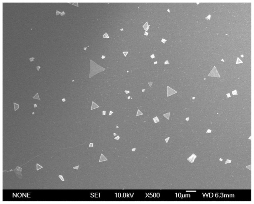
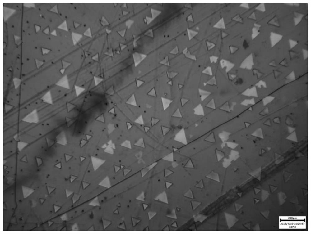
[0062] This example is basically the same as Example 1, except that the substrate in step (1) is mica, and other growth parameters remain unchanged. Due to the good insulation and layered structure of mica, it is more conducive to obtaining regular Cs 3 Bi 2 Br 9 Perovskite microdisks. image 3 For adopting the Cs prepared in Example 2 3 Bi 2 Br 9 The optical microscope photo of the perovskite microdisk, the microdisk is composed of a large number of regular triangles, the size of the triangles is distributed in the range of 15-100 microns, and the average size is obviously larger than the sample obtained in Example 1. Figure 4 For adopting the Cs prepared in Example 2 3 Bi 2 Br 9The scanning electron microscope photo of the perovskite microdisk, from which it can be observed that the surface of a single microdisk is very smooth and flat, the boundary is very steep, and there are no obvious defects.


PUM

PropertyMeasurementUnit
thicknessaaaaaaaaaa
sizeaaaaaaaaaa
sizeaaaaaaaaaa

Abstract

The invention discloses an inorganic non-lead caesium bismuth halogen Cs3Bi2X9 perovskite micrometer disc and a synthesis method thereof. The synthesis method comprises the following steps: (1) cleaning a liner; (2) preparing mixed powder of CsX and BiX3, wherein X=Cl, Br, or I; (3) putting the cleaned liner and the prepared mixed powder into a double-temperature zone horizontal tubular furnace; (4) setting the temperature, the temperature keeping time and the pressure intensity of the horizontal tubular furnace; (5) introducing high-purity argon as a carrier gas, thereby obtaining the inorganic non-lead caesium bismuth halogen Cs3Bi2X9 perovskite micrometer disc. The inorganic non-lead caesium bismuth halogen Cs3Bi2X9 perovskite micrometer disc disclosed by the invention is regular in shape, good in crystallization property, high in stability, and capable of solving the problems that the conventional lead-based perovskite material has toxicity and is easy to decompose in an atmosphereenvironment, and can be applied to preparation of novel photoelectric devices.

Description

technical field [0001] The invention belongs to the field of photoelectric material preparation, in particular to an inorganic non-lead cesium bismuth halide Cs 3 Bi 2 x 9 Perovskite microdisks and methods for their synthesis. Background technique [0002] In recent years, metal halide perovskite materials have attracted widespread attention in the field of new optoelectronic devices due to their excellent optoelectronic properties, including solar cells, light-emitting diodes, lasers, and photodetectors. The general chemical formula of this material is ABX 3 , where A is methylammonium (CH 3 NH 3 , MA), formamidine (CH(NH 2 ) 2 , FA) or metal Cs; B is usually metal Pb; X is Cl, Br or I. However, the organic-inorganic hybrid perovskite system (MAPbX 3 、FAPbX 3 ) has poor stability and is very sensitive to environmental water, oxygen and heat, so that raw material storage and device preparation must be carried out under the protection of inert gas, and the requireme...

Claims


Application Information

Patent Timeline
Patent Type & Authority Patents(China)
IPC IPC(8): C01G29/00B82Y30/00
CPCB82Y30/00C01G29/006C01P2004/03C01P2004/61
Inventor 史志锋李营梁文晴马壮壮张飞
Owner ZHENGZHOU UNIV
Learn More