Chip-original wafer adjustable processing device

A processing device and adjustable technology, applied in the direction of electrical components, semiconductor/solid-state device manufacturing, circuits, etc., can solve the problem of inability to place original chips of different sizes, and achieve the effect of simple structure, convenient operation, and improved adaptability

Active Publication Date: 2018-12-28
泸州龙芯微科技有限公司
View PDF6 Cites 0 Cited by
  • Summary
  • Abstract
  • Description
  • Claims
  • Application Information

AI Technical Summary

Problems solved by technology

[0004] The present invention intends to provide an adjustable processing device for original chips to so

Method used


Image

  • Chip-original wafer adjustable processing device
  • Chip-original wafer adjustable processing device
  • Chip-original wafer adjustable processing device

Examples


Embodiment Construction

[0022] The following is further described in detail through specific implementation methods:

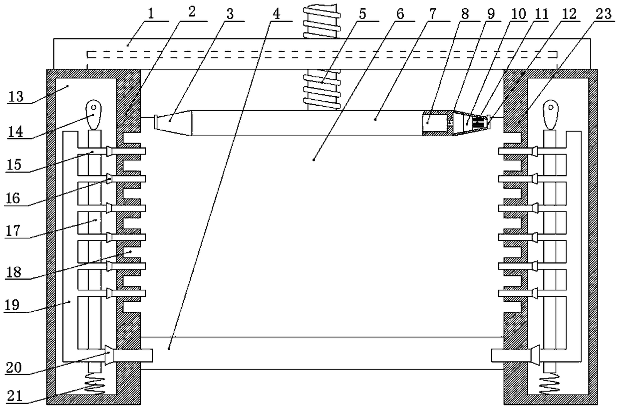
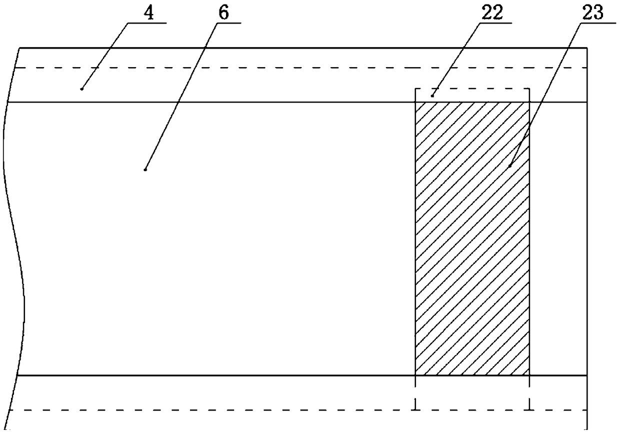
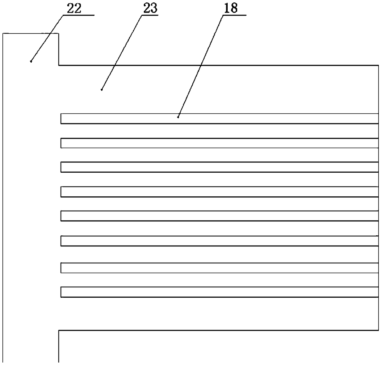
[0023] The reference signs in the drawings of the description include: top plate 1, left side plate 2, collar 3, back plate 4, lead screw 5, first chute 6, turntable 7, water storage chamber 8, water outlet 9, flexible ring 10. Bristles 11, cover plate 12, cavity 13, cam 14, branch pipe 15, one-way outlet valve 16, partition 17, card slot 18, main pipe 19, one-way intake valve 20, spring 21, protrusion 22, Right side panel 23.

[0024] Such as figure 1 and Figure 4 As shown, the adjustable chip processing device of the present invention includes a vertically arranged backboard 4, a left sideboard 2 is installed on the left side of the backboard 4, a right sideboard 23 is installed on the right side of the backboard 4, and a left sideboard 2 is installed on the right side of the backboard 4. And the right side plate 23 is all perpendicular to the back plate 4. Such as figure 1 A...


PUM


Abstract

The invention relates to the technical field of chip processing, in particular a chip-original wafer adjustable processing device, which includes a vertically arranged back plate, a left side plate isarranged on one side of the back plate, a right side plate is arranged on the other side of the back plate, the left and right plates are perpendicular to the back plate. The top of the back plate isprovided with a top plate, and the back plate, the top plate, the left side plate and the right side plate define a placement cavity for placing an original wafer, a plurality of clamping grooves arearranged on the inner side of the left side plate and the inner side of the right side plate, a first sliding groove is arranged on the back plate, a protrusion is arranged at the end of the right side plate, and the protrusion is slidably connected in the first sliding groove, a second sliding groove is arranged on the bottom of the top plate, a magnet is arranged in the second sliding groove, and an iron sliding block is arranged on the top of the right side plate, and the sliding block is slidably connected in the second sliding groove. The invention solves the problem that the original chip with different sizes cannot be placed in the shelf size in the prior art.

Description

technical field [0001] The invention relates to the technical field of chip processing, in particular to an adjustable processing device for an original chip. Background technique [0002] Chips are also called microcircuits, microchips, and integrated circuits. They contain integrated circuits. Chips are small in size and are an important part of computers and other electronic devices. [0003] Existing chips are usually integrated on a large piece of original chip. When using the chip, it needs to be transferred from the original chip. During the processing of the chip, the original chip needs to be processed in advance, such as cleaning and drying. In the prior art, a rack is often used to store the original chips, and the original chips are stacked and inserted into the slots of the rack, and then the entire rack is placed in an oven for drying. The size of the existing racks is fixed and cannot be adjusted, and can only store one size of chip originals. Chips of differ...

Claims


Application Information

Patent Timeline
IPC IPC(8): H01L21/67
CPCH01L21/67011H01L21/67155
Inventor 罗云红
Owner 泸州龙芯微科技有限公司
Why Eureka
Try Eureka