Solder paste printing method

A printing method and technology of the first printing area, applied in the directions of printing, printing devices, etc., can solve the problems of high cost, residual solder paste, poor printing effect, etc., so as to solve the limitation, improve the printing effect, and reduce the process cost. Effect

Active Publication Date: 2019-01-01
李孝鹏
View PDF10 Cites 3 Cited by
  • Summary
  • Abstract
  • Description
  • Claims
  • Application Information

AI Technical Summary

Problems solved by technology

[0004] However, the production process of the stepped stencil is complicated and the cost is high; the printing effect is not good, if the area of ​​the thin area of ​​the stepped stencil is too small, it will easily cause solder paste residue in this area

Method used


Image

  • Solder paste printing method
  • Solder paste printing method
  • Solder paste printing method

Examples


Embodiment Construction

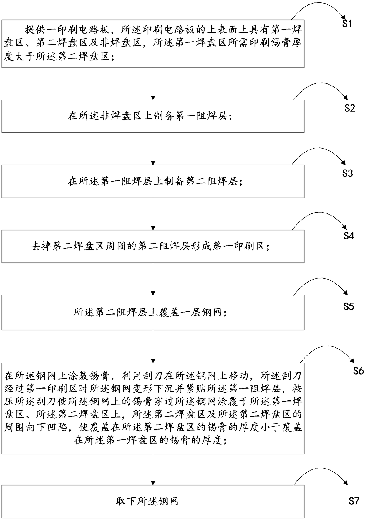
[0030] In order to make the objectives, technical solutions and beneficial technical effects of the present invention clearer, the technical solutions in the embodiments of the present invention will be clearly and completely described below in conjunction with the drawings in the embodiments of the present invention. Obviously, the described implementation Examples are only some embodiments of the present invention, not all embodiments. Based on the embodiments of the present invention, all other embodiments obtained by persons of ordinary skill in the art without making creative efforts belong to the protection scope of the present invention.

[0031] as attached figure 1 Shown, a kind of printing method of solder paste, it comprises the steps:

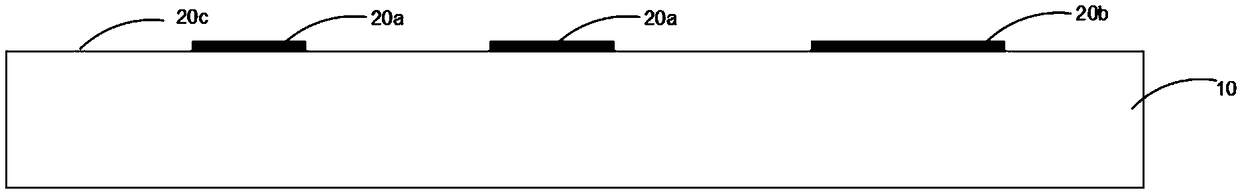
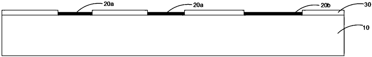
[0032] Step S1: provide a printed circuit board 10, the upper surface of the printed circuit board 10 has a first pad area 20a, a second pad area 20b and a non-pad area 20c, the first pad area 20a The thickness of the solder paste...


PUM


Abstract

The invention provides a solder paste printing method. A preparation method comprises the following specific steps: a printed circuit board is provided; a first welding disc area, a second welding disc area and a non-welding disc area are arranged on the upper surface of the printed circuit board; the thickness of printed solder paste needed by the first welding disc area is larger than the secondwelding disc area; a first welding stop layer is prepared on the non-welding disc area; a second welding stop layer is prepared on the first welding stop layer; the second welding stop layer around the second welding disc area is removed to form a first printing area; a steel net is used for covering; the solder paste is coated on the steel net; a scraper moves on the steel net, and is deformed for sinking when passing through the first printing area and tightly bonded on the first welding stop layer; the scraper is pressed to enable the solder paste to penetrate through the steel net to coaton the first welding disc area and the second welding disc area; the second welding disc area and the periphery of the second welding disc area are recessed down, so that the thickness of the solderpaste covering the second welding disc area is smaller than he thickness of the solder paste covering the first welding disc area; and the steel net is taken down to finally prepare the solder paste with different thicknesses on the same printed circuit board.

Description

technical field [0001] The invention relates to a printed circuit board assembly process, in particular to a printing method of solder paste. Background technique [0002] In the process of manufacturing electronic products, it is necessary to use surface mount technology (SMT) to solder various components to the printed circuit board. The more commonly used surface mount process is: first, the side of the printed circuit board that needs to mount components Apply solder paste on the parts that need to be mounted, and then paste the components that need to be soldered to the corresponding positions of the printed circuit board. After completing the mounting of the components, reflow soldering is performed, which completes the printed circuit board. The placement of components on one side can be completed after passing the inspection. [0003] The stencil is a special mold for surface mount technology. Its main function is to help the deposition of solder paste. The purpose ...

Claims


Application Information

Patent Timeline
Patent Type & Authority Applications(China)
IPC IPC(8): B41M1/12
CPCB41M1/12
Inventor 不公告发明人
Owner 李孝鹏
Why Eureka
Try Eureka