Preparation method of micro-channel plate and micro-channel plate prepared by preparation method

A microchannel plate and columnar technology, which is applied in separation methods, chemical instruments and methods, discharge tube/lamp manufacturing, etc., can solve the difficulty of making uniform film materials on the inner wall of microchannels, substrate deformation, and large aspect ratio holes. Micro-hole etching and other issues, to achieve the effect of excellent structure and device performance, low cost, and avoid material limitation

Pending Publication Date: 2022-05-13
NO 12 RES INST OF CETC
View PDF2 Cites 0 Cited by
  • Summary
  • Abstract
  • Description
  • Claims
  • Application Information

AI Technical Summary

Problems solved by technology

[0012] Based on the above facts, the object of the present invention is to provide a method for preparing a microchannel plate and a microchannel plate prepared by the method, so as to solve the problem of large aspect ratio holes and microscopic holes in the preparation process of the microchannel plate in the prior art. Hole etching, deformation of the substrate after high-temperature treatment for a long time, and difficulty in making uniform thin-film materials on the inner wall of the microchannel

Method used


Image

  • Preparation method of micro-channel plate and micro-channel plate prepared by preparation method
  • Preparation method of micro-channel plate and micro-channel plate prepared by preparation method
  • Preparation method of micro-channel plate and micro-channel plate prepared by preparation method

Examples


preparation example Construction

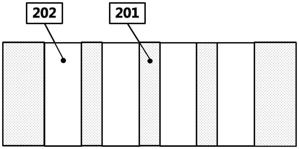
[0050] According to a specific embodiment of the present invention, a kind of preparation method of microchannel plate is provided, such as Figure 3a-3f , including the following steps:

[0051] 1) Provide a substrate 301 .

[0052] The substrate 301 suitable for this embodiment can be a smooth and flat substrate. Exemplary substrates 301 include, but are not limited to, surface-polished silicon wafers, metal sheets, glass sheets, or flatness and roughness that meet micromachining, especially photolithography processes. Other materials required.

[0053] The size of the substrate 301 is preferably a micro-processing standard size, such as 2 inches, 3 inches, 4 inches, 6 inches, or a standard substrate and non-standard substrate larger than 6 inches that can be achieved by micro-processing.

[0054] A suitable thickness of the substrate 301 is preferably 400-2000 microns.

[0055] 2) forming a columnar array 302 at a preselected position on one surface of the substrate 301,...

Embodiment 1

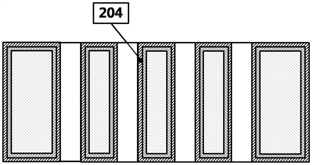
[0090] A microchannel plate, as shown in FIG. 3 , includes an electron multiplication layer 401 , a microchannel plate substrate 402 , an electron transmission channel 403 , an input electrode 404 and an output electrode 405 .

[0091] Its preparation method comprises the following steps:

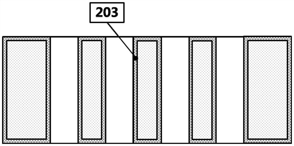
[0092]1) Choose crystal-oriented polished silicon wafer as the substrate 301, the diameter of the silicon wafer is 4 inches, the thickness is 500 microns, the surface flatness and warpage are better than 10 microns; the surface of the silicon wafer is thermally oxidized with 0.5 micron silicon dioxide and magnetron Sputter 1 micron metal aluminum, through standard photolithography, etch silicon dioxide and metal aluminum as a mask layer; use Bosch patented deep silicon etching technology of STS company, etch silicon substrate to form columnar array 302; etching power 600W / 15W, etching rate 1.5μm / min, etching time 200min, etching depth 300μm; according to the design pattern, a dense hexago...

Embodiment 2

[0099] A microchannel plate includes an electron multiplication layer 401 , a microchannel plate substrate 402 , an electron transmission channel 403 , an input electrode 404 and an output electrode 405 .

[0100] Its preparation method is with embodiment 1, and difference is:

[0101] In step 1), select crystal direction polished silicon wafer as the substrate 301, the diameter of the silicon wafer is 4 inches, the thickness is 500 microns, and the surface flatness and warpage are better than 10 microns; 300 microns are spin-coated on the surface of the substrate 301 with 800 RPM Thickness SU8-2150 photoresist, pre-baked at 95°C for 60 minutes, according to the design pattern 600mJ / cm 2 Dose exposure, post-bake at 95°C for 60 minutes, develop with SU8Developer for 45 minutes, and obtain a dense hexagonal columnar array 302 on the silicon wafer. aspect ratio 20.

[0102] In step 3), the chemical vapor deposition method is used to deposit silicon dioxide in the gap between t...


PUM

PropertyMeasurementUnit
heightaaaaaaaaaa
thicknessaaaaaaaaaa
thicknessaaaaaaaaaa

Abstract

The invention discloses a microchannel plate and a preparation method thereof. The preparation method comprises the following steps: providing a substrate; forming a cylindrical array at a preselected position on one surface of the substrate; depositing an electron multiplication material on the surfaces of the substrate and the cylindrical array to form an electron multiplication layer; an insulating material is applied to the electron multiplication layer until the cylindrical array is completely covered, and an insulating layer is formed; grinding and polishing the surface of the insulating layer in the obtained structure until the top end of the cylindrical array is exposed; removing the substrate, and grinding and polishing the surface, combined with the substrate, in the structure until the bottom end of the cylindrical array is exposed; removing the cylindrical array to obtain an insulating layer structure which is provided with a through hole and is coated with an electron multiplication layer on the through hole; and respectively depositing conductive materials on the upper surface and the lower surface of the insulating layer structure except the through holes. The problems of large depth-to-width ratio micropore etching, base material high-temperature long-time treatment deformation and difficulty in uniform manufacturing of micro-channel inner wall film materials in the preparation process of the micro-channel plate are solved.

Description

technical field [0001] The invention relates to the technical field of vacuum electronics. More specifically, it relates to a preparation method of a microchannel plate and a microchannel plate prepared by the preparation method. Background technique [0002] Micro-channel plate is a two-dimensional channel type electron multiplier, which has the advantages of high gain, high resolution, low noise, low power consumption, and long life. It is widely used in low-light image tubes, photomultiplier tubes, cathode ray tubes, camera Tubes and X-ray detectors etc. [0003] The main body of traditional microchannel plate preparation is based on the glass tube stretching technology: lead silicate glass tube is used as the channel glass, an acid-soluble glass rod core is inserted inside the glass tube, and the glass tubes are densely packed and compressed horizontally and stretched longitudinally. Cut into thin slices to form slabs, the slabs are ground and polished, the glass rod c...

Claims


Application Information

Patent Timeline
Patent Type & Authority Applications(China)
IPC IPC(8): H01J43/24H01J9/02B81B1/00B81C1/00
CPCH01J43/246H01J9/02B81C1/00119B81C1/00531B81B1/004B81C2201/0111
Inventor 李兴辉陈海军蔡军
Owner NO 12 RES INST OF CETC
Why Eureka
Try Eureka