Boundary spacer structure and integration

A spacer and boundary technology, applied in semiconductor devices, electrical components, circuits, etc., can solve problems such as limiting device performance

Active Publication Date: 2021-11-05
GLOBALFOUNDRIES INC
View PDF4 Cites 0 Cited by
  • Summary
  • Abstract
  • Description
  • Claims
  • Application Information

AI Technical Summary

Problems solved by technology

However, this in turn results in significantly smaller EPI volumes than desired, limiting device performance

Method used


Image

  • Boundary spacer structure and integration
  • Boundary spacer structure and integration
  • Boundary spacer structure and integration

Examples


Embodiment Construction

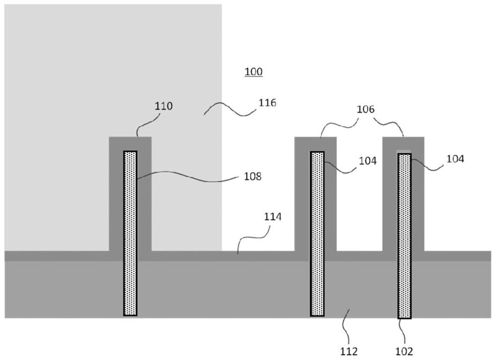
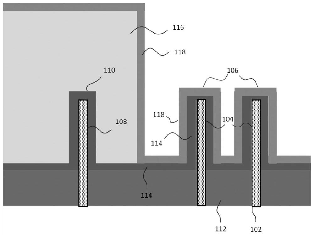
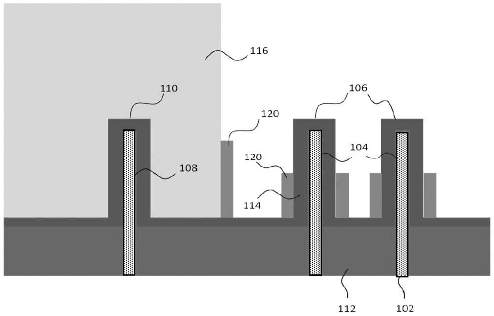
[0015] The present disclosure relates to semiconductor structures, and more particularly, to boundary spacer structures and methods of fabrication for use with FinFET devices. More specifically, the present disclosure provides physical boundaries in the form of barrier layers between fin structures of adjacent devices (eg, PFETs and NFETs) to prevent merging of epitaxial layers in spaces between adjacent fin structures. Advantageously, in an embodiment, a barrier layer between adjacent fin structures will prevent the epitaxial layers from merging together causing short circuits in the device. In addition, the boundary prevents the epitaxial layer of one fin structure from shorting to the Vdd supply line of an adjacent fin structure.

[0016] In a more specific embodiment, in the present disclosure, a mask is formed over the first fin structure on the first device, and a barrier material is formed over the mask and the exposed second fin structure of the second device. Portion...


PUM


Abstract

The present disclosure relates to semiconductor structures, and more particularly, to N-P boundary spacer structures for use with FinFET devices and methods of fabrication thereof. The method includes: forming a plurality of first fin structures; forming a barrier layer between a first fin structure of the plurality of fin structures and a second fin structure of the plurality of fin structures; and forming an epitaxial material on the first fin structures , while blocking the extension of the epitaxial material onto the second fin structure at least by the barrier layer formed between the first fin structure and the second fin structure.

Description

technical field [0001] The present disclosure relates to semiconductor structures, and more particularly, to boundary spacer structures and methods of fabrication for use with FinFET devices. Background technique [0002] As technology nodes advance, a smaller and smaller space is provided between the n-EPI layer and the p-EPI layer formed on adjacent fin structures. For example, in a 7nm structure, the space for n-EPI and p-EPI is typically only about 50nm or less. This small separation can result in N-P shorts between n-EPI and p-EPI or between n-EPI and the Vdd power plane for adjacent devices. For example, during an epitaxial growth process performed on adjacent fins, the dimensions of the epitaxial growth may vary, or anomalous epitaxial growth may occur that expands beyond the mask formed on the respective fins, resulting in amalgamation of the epitaxial material. [0003] The solution to this problem is to reduce the growth time to form the epitaxial layer on the fi...

Claims


Application Information

Patent Timeline
Patent Type & Authority Patents(China)
IPC IPC(8): H01L29/78H01L21/336H01L29/423
CPCH01L29/42364H01L29/66477H01L29/7855H01L21/823814H01L21/823821H01L21/823864H01L21/823878H01L21/02178H01L27/0924H01L29/0653H01L29/0847
Inventor J·R·霍尔特亓屹罗先庆彭建伟
Owner GLOBALFOUNDRIES INC
Why Eureka
Try Eureka