A kind of electrochromic device and preparation method thereof

A technology of electrochromic devices and electrochromic layers, applied in the direction of instruments, nonlinear optics, optics, etc., can solve problems such as easy generation of pinholes or impurities, low ion conductivity, damage to device life, etc., to achieve easy operation, The preparation technology is mature and the effect of reducing leakage current

Active Publication Date: 2021-09-28
CHINA BUILDING MATERIALS ACAD
View PDF5 Cites 0 Cited by
  • Summary
  • Abstract
  • Description
  • Claims
  • Application Information

AI Technical Summary

Problems solved by technology

At present, no electrochromic glass with excellent performance and stable discoloration has been put into the market in large quantities. Second, it is easy to produce pinholes or impurities during the preparation process. These defects cause very serious leakage current, which leads to a sharp increase in power consumption when maintaining the colored state, and seriously damages the life of the device in the long run.

Method used


Image

  • A kind of electrochromic device and preparation method thereof
  • A kind of electrochromic device and preparation method thereof
  • A kind of electrochromic device and preparation method thereof

Examples


preparation example Construction

[0039] The preparation method of the above-mentioned electrochromic device includes the following steps: sequentially depositing an electrochromic layer, an electrolyte layer, an ion storage layer and a second transparent conductive layer on the substrate deposited with the first transparent conductive layer, to obtain the obtained electrochromic device. Wherein the electrochromic layer is deposited on the first transparent conductive layer.

[0040] The electrolyte layer is obtained by sputtering deposition, plasma enhanced chemical vapor deposition, diffusion, ion implantation or epitaxy.

[0041] The present invention is further described below in conjunction with example.

example 1

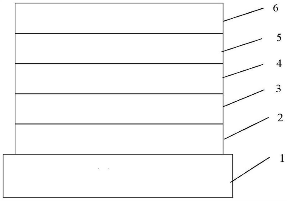
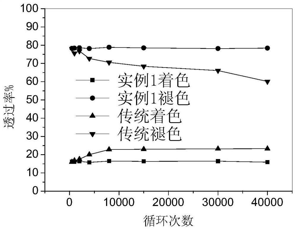
[0043] Such as figure 1 As shown, the example of the present invention provides an electrochromic device, and the electrochromic device comprises a substrate 1 and a first transparent conductive layer 2 deposited on the substrate 1 in sequence, an electrochromic layer 3, an electrolyte Layer 4, ion storage layer 5 and second transparent conductive layer 6; the thickness of the substrate 1 is 2mm; the second transparent conductive layer 2 and the second transparent conductive layer 6 are tin-doped indium oxide (ITO) thin films , its surface resistance is 30Ω / cm 2 , a thickness of 300nm; the electrochromic layer 3 is a tungsten oxide (WO3) film with a thickness of 300nm, the ion storage layer 5 is a nickel-tungsten oxide film with a thickness of 200nm; the electrolyte layer is a PN junction film, It is composed of an N-type semiconductor doped region and a P-type semiconductor doped region; the thickness of the electrolyte layer 4 is 10nm, and its transmittance in the visible l...

example 2

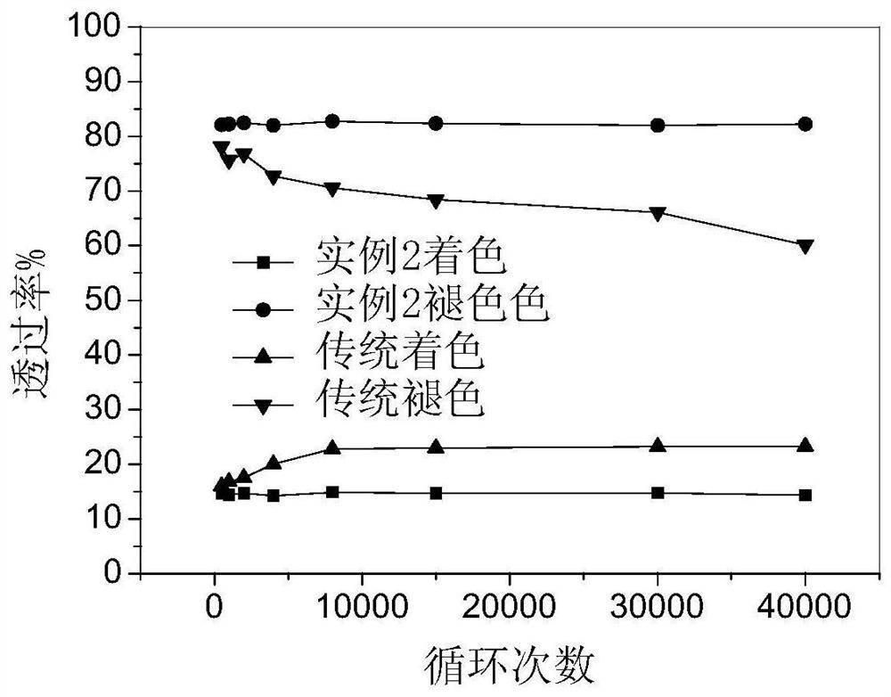
[0054] Such as figure 1 As shown, the example of the present invention provides an electrochromic device, and the electrochromic device comprises a substrate 1 and a first transparent conductive layer 2 deposited on the substrate 1 in sequence, an electrochromic layer 3, an electrolyte Layer 4, ion storage layer 5 and second transparent conductive layer 6; the thickness of the substrate 1 is 2mm; the first transparent conductive layer 2 and the second transparent conductive layer 6 are fluorine-doped tin oxide (FTO) films , its surface resistance is 30Ω / cm 2 , with a thickness of 300nm; the electrochromic layer 3 is a tungsten oxide film, and the ion storage layer 5 is a nickel-tungsten oxide film; the electrolyte layer is a PN junction film, which consists of an N-type semiconductor doped region and a Consists of a P-type semiconductor doped region; the thickness of the electrolyte layer 4 is 100nm, and its transmittance in the visible light range is greater than 80%; the el...


PUM

PropertyMeasurementUnit
thicknessaaaaaaaaaa
surface resistanceaaaaaaaaaa
thicknessaaaaaaaaaa

Abstract

The invention relates to an electrochromic device, which includes a substrate and a first transparent conductive layer, an electrochromic layer, an electrolyte layer, an ion storage layer and a second transparent conductive layer deposited on the substrate in sequence. layer; the electrolyte layer is a PN junction film, which is composed of an N-type semiconductor doped region and a P-type semiconductor doped region. The invention also provides a preparation method of the above-mentioned electrochromic device. The electrochromic device of the present invention utilizes the principle that the PN junction conducts electricity in the forward direction and the reverse resistance is large. Under the forward working voltage, the barrier layer in the PN junction becomes narrower, and the diffusion becomes easier, and the electrochromic The coloring of the electrochromic layer occurs rapidly, reducing the coloring time; when no voltage is applied or a small reverse voltage is applied, the leakage current is greatly reduced due to the large resistance, thereby significantly prolonging the coloring time of the electrochromic layer. The device has fast coloring and obvious open-circuit memory effect, which greatly prolongs the cycle life of the electrochromic glass.

Description

technical field [0001] The invention relates to an electrochromic device, in particular to an electrochromic device with obvious memory effect and a preparation method thereof. Background technique [0002] The phenomenon of electrochromism refers to the phenomenon that the material is accompanied by H under the action of an external electric field. + , Li + 、Na + The electrochemical reaction process occurs when the plasma is injected or extracted, and its optical properties are reversibly changed, thereby realizing the regulation of light reflection, transmission, and absorption. Devices made of electrochromic materials are called electrochromic devices. Electrochromic devices have the advantages of high efficiency, low consumption, no pollution, and intelligence. All have broad application prospects. Electrochromic glass is a commonly used electrochromic device, in which the electrolyte layer of electrochromic glass is the transmission channel for ions required for ele...

Claims


Application Information

Patent Timeline
Patent Type & Authority Patents(China)
IPC IPC(8): G02F1/15G02F1/153
CPCG02F1/15G02F1/1523G02F1/153G02F1/1533
Inventor 孟政刘静汪洪
Owner CHINA BUILDING MATERIALS ACAD
Why Eureka
Try Eureka