Pixel compensation circuit, driving method thereof, and display device

A technology for compensating circuits and pixels, applied in static indicators, instruments, etc., can solve the problem of reducing the impact of pixel size, and achieve the effect of reducing size and simplifying structure

Active Publication Date: 2019-01-04
EVERDISPLAY OPTRONICS (SHANGHAI) CO LTD
View PDF10 Cites 2 Cited by
  • Summary
  • Abstract
  • Description
  • Claims
  • Application Information

AI Technical Summary

Problems solved by technology

At present, most of the existing pixel compensation circuits need to be composed of more than 6 thin film transistors, so it has a certain impact on the reduction of the pixel size.

Method used


Image

  • Pixel compensation circuit, driving method thereof, and display device
  • Pixel compensation circuit, driving method thereof, and display device
  • Pixel compensation circuit, driving method thereof, and display device

Examples


Embodiment Construction

[0028] The technical content of the present invention will be further described below in conjunction with the accompanying drawings and embodiments.

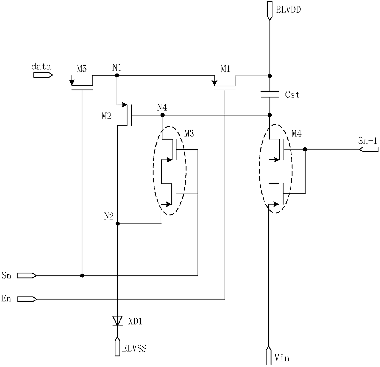
[0029] See figure 1 , which shows a schematic circuit diagram of a pixel compensation circuit of the present invention. In an embodiment of the present invention, the pixel compensation circuit includes a switch module, a drive module, a compensation module, an initialization module, a data gating module, a voltage storage module and a light emitting element. Wherein, the switch module, the drive module, the compensation module, the initialization module and the data gating module all include a first terminal, a second terminal and a control terminal.

[0030] The first end of the switch module is connected to the first external power supply, and the second end of the switch module is respectively connected to the first end of the drive module for controlling the opening and closing of the circuit between the first power supply...


PUM


Abstract

The invention discloses a pixel compensation circuit, a driving method thereof and a display device. The pixel compensation circuit includes a first transistor, a driving transistor, a third transistor, a fourth transistor, a fifth transistor, a storage capacitor and a light emitting component; the first end of the first transistor is connected with a first power source; the second end of the first transistor is connected with a first node; the control end of the first transistor is connected with a control signal line; the first end of the driving transistor is connected with the first node;the second end of the driving transistor is connected with a second node; the control end of the driving transistor is connected with a fourth node; the third transistor is connected with the drivingtransistor; the control end of the third transistor is connected with an external first scanning signal line; the first end of the fourth transistor is connected with a fourth node; the second end ofthe fourth transistor is connected with a second power source; the control end of the fourth transistor is connected with an external second scanning signal line; the first end of the fifth transistoris connected with the driving transistor; the second end of the fifth transistor is connected with a data signal line; the control end of the fifth transistor is connected with the first scanning signal line; the first end of the storage capacitor is connected with the first power source; the second end of the storage capacitor is connected with the fourth node; the anode of the light emitting component is connected with the second node; and the cathode of the light emitting component is connected with a third power source.

Description

technical field [0001] The present invention relates to the field of display technology, in particular to a pixel compensation circuit, a driving method thereof, and a display device with the pixel compensation circuit. Background technique [0002] Compared with traditional liquid crystal displays, organic light-emitting display panels have the advantages of fast response, high contrast, brilliant colors, higher resistance to high and low extreme temperatures, and thinner and lighter weight. Therefore, they have gradually become the mainstream technology in the display field and are widely used in mobile phones, Tablet PCs, TVs, virtual reality, and more. [0003] Although the organic light-emitting display panel has the above-mentioned advantages, many problems arise during its application. For example, since the luminance of an organic light-emitting display device is related to the magnitude of the current flowing through the organic light-emitting display device, the e...

Claims


Application Information

Patent Timeline
Patent Type & Authority Applications(China)
IPC IPC(8): G09G3/3233
CPCG09G3/3233
Inventor 周兴雨
Owner EVERDISPLAY OPTRONICS (SHANGHAI) CO LTD
Why Eureka
Try Eureka