Check patentability & draft patents in minutes with Patsnap Eureka AI!

A TFT array substrate and a display panel

An array substrate and patterning technology, applied to electrical components, electrical solid devices, circuits, etc., can solve problems such as TFT electrical characteristic deviation, achieve the effect of reducing reaction and improving TFT reliability

Active Publication Date: 2019-01-04
SHENZHEN CHINA STAR OPTOELECTRONICS SEMICON DISPLAY TECH CO LTD
View PDF4 Cites 2 Cited by
  • Summary
  • Abstract
  • Description
  • Claims
  • Application Information

AI Technical Summary

Problems solved by technology

The buffer layer 2, the interlayer insulating layer 6 and the passivation layer 8 are prepared by SiOx, such as figure 1 As shown by the dotted arrow, the hydrogen atoms contained in the buffer layer 2, the interlayer insulating layer 6 and the passivation layer 8 have the opportunity to diffuse into the channel formed by the active layer 3, which will shift the electrical characteristics of the TFT.

Method used


Image

  • A TFT array substrate and a display panel
  • A TFT array substrate and a display panel
  • A TFT array substrate and a display panel

Examples


Embodiment Construction

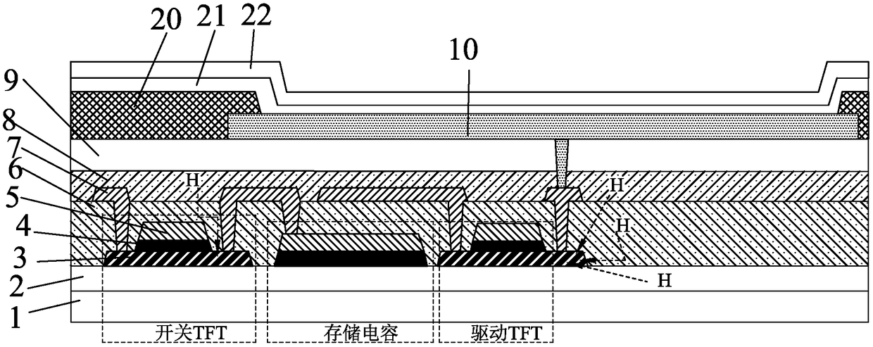
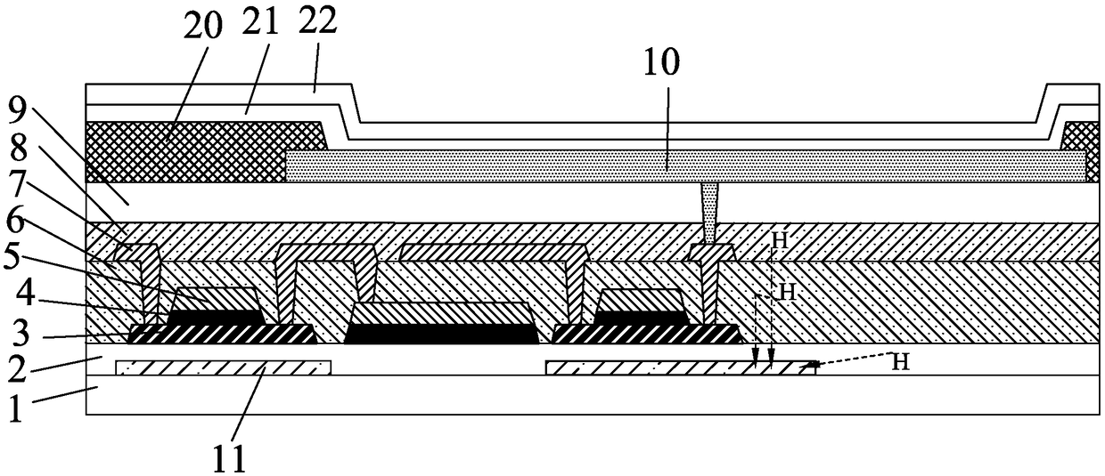
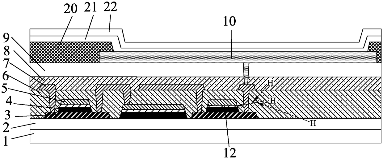
[0026] Similar to a general TFT array substrate, the TFT array substrate of the present invention mainly includes a patterned metal oxide active layer, a gate metal layer, and a source-drain metal layer, through which the metal oxide active layer, the gate metal layer, and The source-drain metal layer can form a metal oxide TFT device; the present invention further includes at least one patterned hydrogen-absorbing metal layer, and the hydrogen-absorbing metal layer reduces the reaction of hydrogen atoms with the active layer of the metal oxide TFT to improve TFT reliability. In addition, a dielectric layer is provided between the hydrogen-absorbing metal layer and the patterned metal oxide active layer, which can separate the metal oxide active layer and the hydrogen-absorbing metal layer. The hydrogen absorbing metal can be titanium metal or nickel alloy metal, or other suitable materials.

[0027] see figure 2 , which is a schematic cross-sectional structure diagram of a ...


PUM


Abstract

The invention relates to a TFT array substrate and a display panel. The TFT array substrate comprises a patterned metal oxide active layer, a gate metal layer, and a source-drain metal layer, and further comprises at least one patterned hydrogen-absorbing metal layer, and a dielectric layer is arranged between the hydrogen-absorbing metal layer and the patterned metal oxide active layer. The TFT array substrate and the display panel of the present invention can reduce the reaction of hydrogen atoms with the metal oxide TFT active layer, thereby achieving the purpose of improving the TFT reliability.

Description

technical field [0001] The invention relates to the field of display technology, in particular to a TFT array substrate and a display panel. Background technique [0002] Metal oxide thin film transistors (Metal oxide TFT) (such as IGZO; IGTO...) have a relatively simple manufacturing process, high carrier mobility, low leakage current and better electrical stability, so they are used in organic light-emitting diodes (OLED) display drive circuit, the disadvantage of metal oxide TFT is that the oxygen atoms in the metal oxide are easily reduced by hydrogen atoms, resulting in oxygen vacancies, which cause the electrical characteristics of TFT to drift. The existing practice is to reduce the source of hydrogen atoms. The dielectric layer material of metal oxide TFT uses SiOx instead of SiNx (such as buffer layer (Buffer layer), interlayer insulating layer (ILD), passivation layer (PV) and other film layers), but according to different chemical vapor deposition (CVD ) film-for...

Claims


Application Information

Patent Timeline
Patent Type & Authority Applications(China)
IPC IPC(8): H01L27/12
CPCH01L27/1214H01L27/1237H01L27/1262H01L27/1225H01L29/7869H01L29/4908H01L27/1255H01L29/78633H10K59/1213H01L29/78606
Inventor 方俊雄吴元均吕伯彦
Owner SHENZHEN CHINA STAR OPTOELECTRONICS SEMICON DISPLAY TECH CO LTD
Features
  • R&D
  • Intellectual Property
  • Life Sciences
  • Materials
  • Tech Scout
  • Unparalleled Data Quality
  • Higher Quality Content
  • 60% Fewer Hallucinations
Learn More