Micro LED transfer method, display panel and display device

A display panel and transfer method technology, applied in the direction of semiconductor devices, electrical components, circuits, etc., can solve the problems of complex detection and repair process, and achieve the effect of simplifying the detection and repair process

Active Publication Date: 2019-01-04
SHANGHAI TIANMA MICRO ELECTRONICS CO LTD
View PDF5 Cites 40 Cited by
  • Summary
  • Abstract
  • Description
  • Claims
  • Application Information

AI Technical Summary

Problems solved by technology

[0005] In view of this, the present invention provides a Micro LED transfer method, a Micro LED display panel, and a Micro LED display device to solve the problem of detecting and repairing after the Micro LED is bonded on the receiving substrate in the prior art, so that subsequent detection and repair more complex issues

Method used


Image

  • Micro LED transfer method, display panel and display device
  • Micro LED transfer method, display panel and display device
  • Micro LED transfer method, display panel and display device

Examples


Embodiment Construction

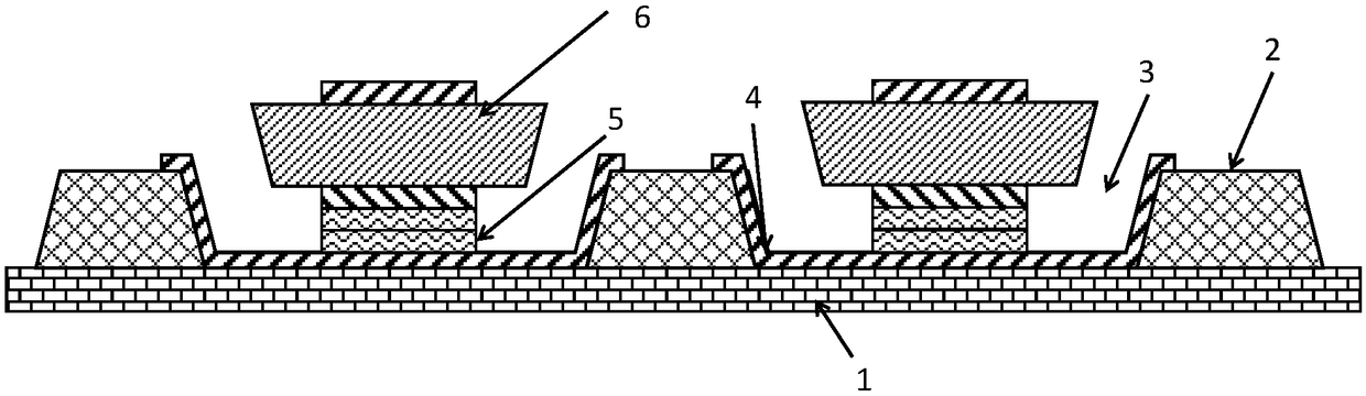
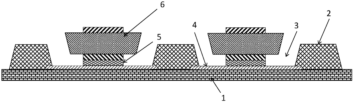
[0044] As mentioned in the background technology, the mass transfer technology of direct transfer or indirect transfer in the prior art detects the Micro LED after bonding the Micro LED on the receiving substrate, and then detects it through the detection circuit. If an abnormal Micro LED is detected, Then replace and repair the abnormal Micro LED, but this makes the subsequent detection and repair process more complicated.

[0045]The inventors found that in the prior art, the direct transfer or indirect transfer of Micro LEDs does not involve the detection of Micro LEDs, but after the transfer of all Micro LEDs is completed, a specific detection process is adopted to detect Micro LEDs. When the Micro LEDs with abnormal display appear, follow-up repair process is adopted to repair the Micro LEDs with abnormal display, for example, the Micro LEDs with redundant transfer are used to replace the Micro LEDs with abnormal Replacement, the replacement of the bonded Micro LED specif...


PUM


Abstract

A Micro LED transfer method, a Micro LED display panel and a Micro LED display device are disclosed. The Micro LED display panel comprises a substrate, a pixel definition layer, and the pixel definition layer comprises an opening, a first conductive layer stacked in the opening, a photosensitive conductive bonding layer and a Micro LED structure. The photosensitive conductive bonding layer has a post-illumination curing, such that structures bonded to opposing surfaces of the photosensitive conductive bonding layer can be bonded together, due to the presence of a photosensitive conductive bonding layer, As that detection of the Micro LED can be realize during the transfer process of the Micro LED, and the subsequent detection is not performed after the bonding is complete, the step of removing the bonded abnormal display Micro LED is saved, and the detection and repair process of the Micro LED is simplified.

Description

technical field [0001] The present invention relates to the field of display technology, in particular to a Micro LED (Micro Light Emitting Diode, micro light emitting diode or micro light emitting diode) transfer method, a Micro LED display panel and a Micro LED display device. Background technique [0002] Micro LED has developed into one of the hotspots of future display technology. The size of LEDs used in Micro LED displays is micron level, with independent control of pixels, independent light emission control, high luminance, low power consumption, ultra-high resolution and high chromaticity, etc. characteristics, but its technical difficulties are many and complex, especially its key technology: mass transfer technology. With the development of technology, mass transfer technology has developed many technical branches, such as electrostatic adsorption, laser and so on. [0003] The traditional mass transfer method of micro-LEDs is to transfer the micro-elements from ...

Claims


Application Information

Patent Timeline
Patent Type & Authority Applications(China)
IPC IPC(8): H01L27/15
CPCH01L27/156H01L25/0753H01L2933/0066H01L33/62H01L25/167H01L33/0095H01L2924/12041H01L24/95H01L2224/95001H01L2924/10155H01L2224/24137H01L24/24H01L33/20H01L24/83H01L2224/83001H01L24/82H01L2224/32145H01L2224/32147H01L24/29H01L24/13H01L24/81H01L2224/16145H01L2224/16147H01L2924/15156H01L2224/7598H01L2224/75303H01L2224/75305H01L24/75H01L2224/2929H01L2224/29339H01L2224/13339H01L2224/1329H01L2924/00012H01L2924/0635H01L2924/00014H01L2924/0675H01L33/36H01L2224/83871H01L2224/8322H01L2224/83234
Inventor 何泽尚邢亮符鞠建刘刚
Owner SHANGHAI TIANMA MICRO ELECTRONICS CO LTD
Why Eureka
Try Eureka