Digital microfluidic chip fault repair method based on combination of improved Dijkstra algorithm and IPSO

A digital micro-flow, fault repair technology, applied in electrical digital data processing, computing, special data processing applications, etc., can solve problems such as long time and low efficiency

Active Publication Date: 2019-01-11
HARBIN INST OF TECH
View PDF12 Cites 10 Cited by
  • Summary
  • Abstract
  • Description
  • Claims
  • Application Information

AI Technical Summary

Problems solved by technology

[0006] The purpose of the present invention is to solve the problems of long time and low efficiency of the existing digital microfluidic chip faul

Method used


Image

  • Digital microfluidic chip fault repair method based on combination of improved Dijkstra algorithm and IPSO
  • Digital microfluidic chip fault repair method based on combination of improved Dijkstra algorithm and IPSO
  • Digital microfluidic chip fault repair method based on combination of improved Dijkstra algorithm and IPSO

Examples


Embodiment Construction

[0065] The following will clearly and completely describe the technical solutions in the embodiments of the present invention with reference to the accompanying drawings in the embodiments of the present invention. Obviously, the described embodiments are only some, not all, embodiments of the present invention. Based on the embodiments of the present invention, all other embodiments obtained by persons of ordinary skill in the art without creative efforts fall within the protection scope of the present invention.

[0066] It should be noted that, in the case of no conflict, the embodiments of the present invention and the features in the embodiments can be combined with each other.

[0067] The present invention will be further described below in conjunction with the accompanying drawings and specific embodiments, but not as a limitation of the present invention.

[0068] The principles involved in the present invention are as follows:

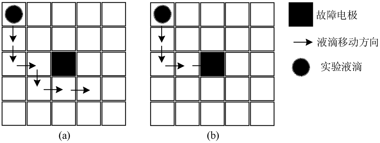
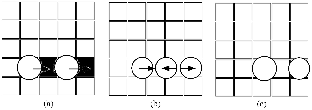
[0069] 1. Digital microfluidic chip d...


PUM


Abstract

A digital microfluidic chip fault repair method based on the combination of improved Dijkstra algorithm and IPSO relates to the field of digital microfluidic chip fault repair, aiming at solving the problems of time consuming and low efficiency of the existing digital microfluidic chip fault repair methods. The method comprises the following steps: first, calculating the shortest path between twodroplets to be mixed based on the improved Dijkstra algorithm; the improved Dijkstra algorithm introduces a cost function into the existing Dijkstra algorithm. The cost function guides the existing Dijkstra algorithm to search in the direction of the shortest distance to the start point, the shortest distance to the end point and the longest distance to the fault point. Step 2, calculating a moving path based on IPSO, so as to realize the shortest moving distance of droplets and complete fault repair under the condition of ensuring the completion of mixing. The invention is suitable for repairing the faults of the digital microfluidic chip.

Description

technical field [0001] The invention relates to the field of digital microfluidic chip fault repair. Background technique [0002] With the development of science and technology, the field of automatic testing has expanded from the testing of analog circuits or digital circuits to the testing of MEMS (Micro-Electromechanical Systems). Microfluidic chip, also known as Lab-on-a-chip, can complete various functions of biological laboratory and routine chemical testing on a chip of a few square centimeters. It has the characteristics of miniaturization, high sensitivity, low cost, and integration. The first generation of microfluidic biochips has permanently etched microvalves, micropumps, and microchannels, and the specific operations are based on continuous fluid flow. The development of microfluidic technology and manufacturing process has promoted the generation of digital microfluidic chips, which manipulate discrete droplets on two-dimensional microfluidic arrays and hav...

Claims


Application Information

Patent Timeline
IPC IPC(8): G06F17/50
CPCG06F2111/06G06F30/392G06F30/367
Inventor 郑文斌付平石金龙尹洪涛王安琪叶俊涛孙媛媛
Owner HARBIN INST OF TECH
Why Eureka
Try Eureka