Vacuum chuck

A vacuum suction cup, suction cup technology, applied in electrical components, semiconductor/solid-state device manufacturing, circuits, etc., can solve the problems of decreased bonding accuracy and increased wafer spacing, and achieve the effect of improving wafer bonding accuracy

Inactive Publication Date: 2019-02-01
YANGTZE MEMORY TECH CO LTD
View PDF3 Cites 3 Cited by
  • Summary
  • Abstract
  • Description
  • Claims
  • Application Information

AI Technical Summary

Problems solved by technology

This will lead to a corresponding increase in the distance between the two bonded wafers, and the increase in the distance between the two wafers will inevitably lead to a decrease in bonding accuracy

Method used


Image

  • Vacuum chuck
  • Vacuum chuck
  • Vacuum chuck

Examples


Embodiment Construction

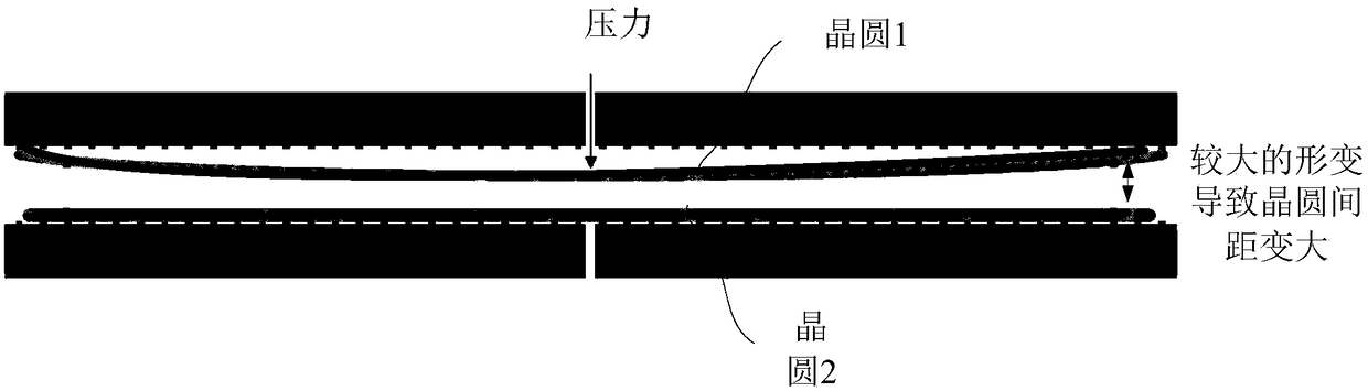
[0033] In the industry, in order to compensate for the size difference between the two wafers to be bonded due to the wafer size change during the wafer processing process, thereby improving the alignment accuracy of wafer bonding, different pressures are usually applied to the wafer through vacuum chucks , however, as figure 1 As shown, the pressure applied to the wafer is not applied uniformly over the entire area of ​​the wafer, but is applied to a local area of ​​the wafer, for example, through a force application point, which is usually located near the center of the wafer, and Each wafer has a certain area, so that different regions of the wafer have the problem of uneven force. Therefore, under the pressure, the wafer will deform in the direction perpendicular to the surface of the wafer, so that the bonded The distance between the two wafers in the wafer edge area increases, which leads to an inevitable decline in bonding accuracy.

[0034] In order to solve the above...


PUM


Abstract

The application discloses a vacuum chuck comprising a chuck body including a fixed central portion and a peripheral portion that can stretch along the radial direction of the chuck body. When a wateris attached to the chuck body, the peripheral portion is controlled to stretch along the radial direction of the chuck body; and the peripheral portion stretching along the radial direction of the chuck body can drive the attached wafer to deform along the radial direction of the chuck body, so that the wafer dimension changes. The wafer with the changed dimension matches the dimension of a to-be-bonded wafer to realize basic consistence of the dimensions of the two wafers. Moreover, the peripheral portion drives the wafer to deform along the plane direction of the wafer to prevent deformationof the wafer along other directions, so that the space between the two to-be-bonded wafers is not changed based on the wafer deformation amount controlling mode. Therefore, the vacuum chuck is able to control the deformation amount of the wafer, so that the bonding precision of wafers is improved.

Description

technical field [0001] The present application relates to the technical field of semiconductor manufacturing equipment, in particular to a vacuum chuck. Background technique [0002] With the development of semiconductor manufacturing technology, wafer bonding technology is more and more widely used in semiconductor manufacturing, and wafer alignment is required in the bonding process. In wafer bonding technology, the alignment accuracy of wafers is directly related to the quality of wafer bonding. Therefore, it is necessary to precisely control the alignment accuracy of wafers. [0003] However, with the development of semiconductor manufacturing technology, the process of wafer processing becomes more and more complicated, which will inevitably lead to changes in wafer size. Although the wafer size variation caused by processing steps is only on the micron scale, the resulting deviation in bond alignment is enough to cause bond failure. [0004] In the prior art, in orde...

Claims


Application Information

Patent Timeline
Patent Type & Authority Applications(China)
IPC IPC(8): H01L21/683H01L21/67
CPCH01L21/67092H01L21/6838
Inventor 刘孟勇丁滔滔刘武邢瑞远陈国良
Owner YANGTZE MEMORY TECH CO LTD
Why Eureka
Try Eureka